Copyright 2000 National Semiconductor Corp.
1
www.national.com
SC14404
Complete Baseband Processor for DECT Handsets
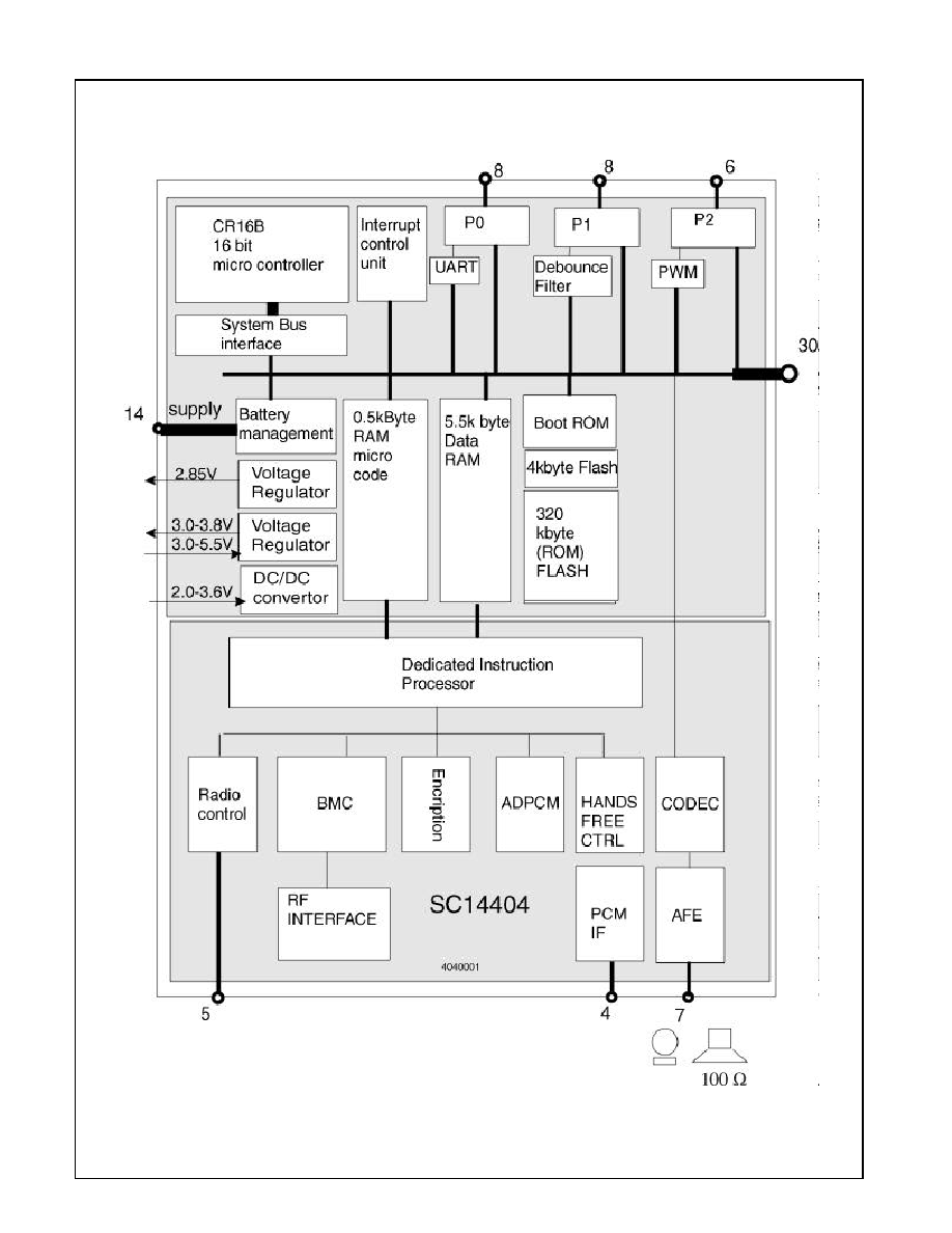
General Description
The SC14404 is a CMOS chip optimized to handle all the
audio, signal and data processing needed within a DECT
handset. An ADPCM transcoder, a very low power CO-
DEC and Analog Frontend is integrated. Direct connec-
tions towards microphone and a (dynamical) loudspeaker
are provided. Duplex quality handsfree operation is inte-
grated.
The SC14404 is designed to fit to any radio design.
A dedicated TDMA controller handles all physical layer
slot formats and radio control.
National Semiconductors standard CompactRISC
TM
CR16B 16 bit microcontroller takes care of all the higher
protocol stack. 4 kilobyte F lash is integrated for parameter
and number storage.
Features
n
Integrated DECT Baseband transceiver optimized for
GAP handsets according to ETS 300 175-2, 175-3 &
175-8.
n
Two on board low drop voltage regulators with 2.85V
and 3.0- 3.8V (with external resistors the voltage can be
determined) output.
n
2V upto 3.6V battery input with onboard step up con-
verter.
n
3V upto 5.0V battery monitor input.
n
Advanced battery management unit
n
Very low power in active and paging mode.
n
Embedded 16 bit CompactRISC
T M
Micro Controller.
(CR16B) with programmable clock speeds.
n
4k byte memory mapped Flash
n
320 kbyte Flash or factory programmed ROM FLASH.
n
ACCESSBUS
TM
or MICROWIRE
T M
interfaces
n
5,5 kilobyte on-chip Data Memory.
n
One full duplex ADPCM transcoder.
n
On-chip 14-bit linear CODEC.
n
14 upto 44 dB gain differential microphone input buffer.
n
100
loudspeaker driver.
n
Software controlled gain on audio input and output.
n
Peak hold ADC for RSSI measurement.
n
Five general purpose inputs can be multiplexed on an
8 bit ADC with selectable ranges.
n
On-chip dedicated TDMA instruction co-processor
which supports 1.152 MHz, 0.576 MHz and 0.288 MHz
bit rates.
n
Seven programmable control signals for radio front
end.
n
Full and double slot, protected and unprotected B-
fields.
n
Duplex quality handsfree operation.
n
Tone generator. Tones consisting of 3 frequencies can
be programmed
n
Linear PCM interface for external codec.
________________________________________________________________________________________________
System Diagram
PRELIMINARY
FEBRUARY 2000
S
C
1
4
4
0
4
C
o
m
p
l
e
t
e
B
a
s
e
b
a
n
d
P
r
o
c
e
s
s
o
r
f
o
r
D
E
C
T
H
a
n
d
s
e
t
s
Note: ACCESSBUS
T M
, MICROWIRE
T M
and CompactRISC
T M
are trade-
marks of National Semiconductor Corporation.
Copyright 2000 National Semiconductor Corp.
2
www.national.com
S
C
1
4
4
0
4
C
o
m
p
l
e
t
e
B
a
s
e
b
a
n
d
P
r
o
c
e
s
s
o
r
f
o
r
D
E
C
T
H
a
n
d
s
e
t
s
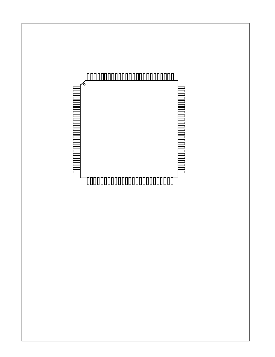
1.0 CONNECTION DIAGRAMS
Order Number SC14404BFLAG (320kbyte Full FLASH, Boot mode A, 100 pins TQFP,
Order Number SC14404BFLBG (320kbyte Full FLASH, Boot mode B, 100 pins TQFP
Order Number SC14404BxxAG (320kbyte ROM FLASH, Boot mode A , 100 pins TQFP)
Order Number SC14404BxxBG (320kbyte ROM FLASH, Boot mode B, 100 pins TQFP)
See NS Package Number VJG100A
AD0
AD1
AD2
AD3
RSTN
AVS2
LRS+
AVD
VDDRF
LRS-
VREF-
MIC-
AGND
MIC+
VREF+
VBAT1
VBAT2
VBAT3
DC_stab
LDO1_CTRL
DC_I
AVS
AD18
CAP
DAC
PD7
PD1
PD5
PD4
PD3
PD2
Xtal1
RFCLK
RSSI
PCM_FSC/PD6/ADC3
PCM_CLK/DAC2/ADC2
VSS
SK
SO
TDO
CMPREF
RDI
LE
VDD
P
0
[
3
]
P
0
[
4
]
P
0
[
5
]
P
0
[
6
]
P
0
[
7
]
P
1
[
0
]
P
1
[
1
]
P
1
[
2
]
P
1
[
3
]
P
1
[
4
]
P
1
[
5
]
P
2
[
5
]
V
D
D
V
S
S
D
C
_
C
T
R
L
P
2
[
0
]
P
2
[
1
]
P
2
[
2
]
1
2
3
4
5
6
7
8
9
10
11
12
13
14
15
16
17
18
19
20
21
22
23
24
25
75
74
73
72
71
70
69
68
67
66
65
64
63
62
61
60
59
58
57
56
55
54
53
52
51
1
0
0
9
9
9
8
9
7
9
6
9
5
9
4
9
3
9
2
9
1
9
0
8
9
8
8
8
7
8
6
8
5
8
4
8
3
8
2
8
1
8
0
7
9
7
8
7
7
7
6
2
6
2
7
2
8 29 30 31 32 33 34 35 36 37 38 39 40 41 42 43 44 45 46 47 48 49 50
SC14404
A
D
4
A
D
5
A
D
6
A
D
1
2
A
D
1
5
A
D
1
6
W
R
n
A
D
1
7
A
D
1
4
A
D
1
3
A
D
9
A
D
1
1
R
D
n
A
D
1
0
R
C
S
n
D
A
B
7
D
A
B
6
D
A
B
5
V
S
S
V
D
D
D
A
B
4
D
A
B
3
D
A
B
2
A
D
8
A
D
7
I
N
T
1
n
I
N
T
0
n
I
N
T
2
n
I
N
T
3
n
I
N
T
4
n
P
O
N
I
N
T
5
n
P
W
M
0
P
C
M
_
D
I
P
W
M
1
A
D
C
0
P
1
[
6
]
P
1
[
7
]
S
C
L
P
2
[
4
]
P
2
[
3
]
P
C
M
_
D
0
A
D
C
1
AVD2
DC_Sense
LDO_Sense
LDO2_CTRL
P
0
[
0
]
P
0
[
1
]
P
0
[
2
]
U
T
X
U
R
X
DAB0
DAB1
P2[6]
C
H
A
R
G
E
S
D
A
DC_DIS
P
2
[
7
]
Copyright 2000 National Semiconductor Corp.
3
www.national.com
S
C
1
4
4
0
4
C
o
m
p
l
e
t
e
B
a
s
e
b
a
n
d
P
r
o
c
e
s
s
o
r
f
o
r
D
E
C
T
H
a
n
d
s
e
t
s
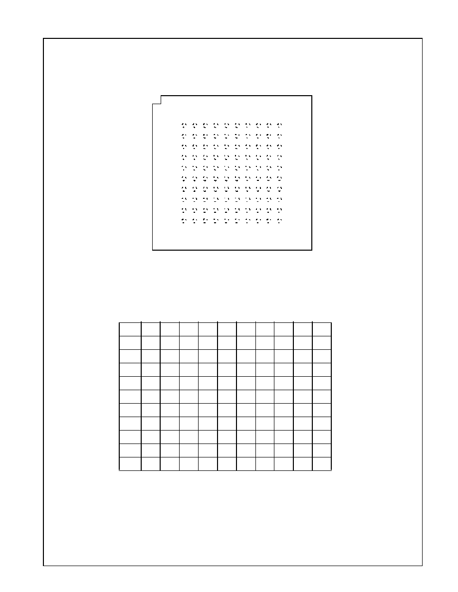
Order Number SC14404BFLBC (320kbyte Full FLASH, Boot mode B, 100 pins CSP
Order Number SC14404BxxBC (320kbyte ROM FLASH, Boot mode B, 100 pins CSP
Note 1: All digital outputs can sink/source 2 mA unless otherwise specified. All digital inputs are Schmitt trigger types. After reset all I/Os are set to input
and all pull-up or pull-down resistors are enabled unless otherwise specified.
PU = Pull-up resistor enabled, PD = Pull-down resistor enabled, I = input
A-I, B-I = In Boot mode A or B input and pull-up or pull-down resistor disabled,
A-PD, B-PU = In Boot mode A, Pull-down resistor enabled. In Boot mode B, pull-up resistor enabled.
Note 2: Reset state of address and data bus and WRn, RDn pins:
If SC14404: Hi-Z/1 means Hi-Z if RSTn is LOW, if RSTn goes HIGH i t takes 32 SCLK cycles = 25 usec before these pin drives a `1'.
Table 1: TQFP pin mapping onto CSP package (See table 2 for TQFP pin description)
1
2
3
4
5
6
7
8
9
10
A
1
99
96
93
89
88
86
85
83
76
B
8
2
98
95
92
90
87
80
77
74
C
10
5
3
97
94
84
82
78
73
71
D
11
12
7
6
100
79
81
72
70
68
E
13
15
9
4
16
91
75
69
67
64
F
14
17
19
25
41
66
54
59
65
63
G
18
20
22
31
29
50
56
57
62
61
H
21
23
28
32
34
44
47
53
55
60
J
24
27
30
37
40
42
45
48
52
58
K
26
33
35
36
38
39
43
46
49
51
1 2 3 4 5 6 7 8 9 10
A
B
C
D
E
F
G
H
J
K
SC14404 CSP pin diagram
(TOP View)
Copyright 2000 National Semiconductor Corp.
5
www.national.com
S
C
1
4
4
0
4
C
o
m
p
l
e
t
e
B
a
s
e
b
a
n
d
P
r
o
c
e
s
s
o
r
f
o
r
D
E
C
T
H
a
n
d
s
e
t
s
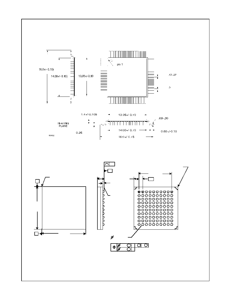
2.0 Package information
FIGURE 2. 100 pins TP Quad Flat Pack. NS Package Number VJG100A
FIGURE 3. 100 pins Chip Scaled Package. NS package SLC100A
1
2
3
4
5
6
7
8
9
10
A
B
C
D
E
F
G
H
J
K
0.8 TYP
(7.2 TYP)
(1.4 TYP)
0.36 +- 0.05 TYP
1.4 0.1
+
-
0.46 TYP
10 0.2
+
-
10 0.2
+
-
A1 BALL PAD CORNER
A1 BALL PAD CORNER
Bottom view
Top view
Dimensions are in milimeters
Note 2
N
Note 3
SEATING PLANE
Note 3
0.1
0.15 M N
0.08 M N
L S M S
NOTES: UNLESS OTHERWISE SPECIFIED
1. SOLDER BALL COMPOSITION: Sn 63%, Pb 37%
2. DIMENSIONS MEASURED AT MAXIMUM SOLDER BALL DIAMETER,
PARALLEL TO PRIMARY DATUM N
3. PRIMARY DATUM N AND SEATING PLANE ARE DEFINED BY THE SPHERICAL
CROWNS OF THE SOLDER BALLS
L
M
4. NO JEDEC REGISTRATION AS OF JUNE 1998