1
- January 1998
Highlights
www.national.com
©
1998 National Semiconductor Corporation
PRELIMINARY
April 1998
PC87570 Keyboard and Power Management Controller
Highlights
General Description
The PC87570 is a highly integrated embedded RISC-based
controller optimized for power management (PM), keyboard
and mouse (KBC) and system control in portable Personal
Computer (PC) applications.
The PC87570 incorporates National's CompactRISC
TM
CR16A core, a high performance 16-bit RISC processor
core, a Bus Interface Unit (BIU) that directly interfaces with
memory and I/O devices, on-chip memory and system sup-
port functions. Among these are legacy functions, handled
by the Host Bus Interface (HBI), that include the Real-Time
Clock and Advanced Power Control (RTC and APC), and
peripherals, including: frequency-multiplier-based High Fre-
quency Clock Generator (HFCG), Power Mode Control
(PMC), Interrupt Control Unit (ICU), Multi-Input Wake-Up
(MIWU), General Purpose I/O Ports (GPIO) with internal
keyboard matrix scanning, PS/2
®
Interface, ACCESS.bus
®
(ACB) Interface, two Multi-Function 16-Bit Timers (MFT16),
periodic interrupt timer and WATCHDOG
TM
(TWD), ADC
and DAC.
The PC87570 highly efficient architecture and its on-chip
peripherals, supporting functions and low power consump-
tion, provide a highly integrated solution for portable note-
book PCs, sub-notebook PCs and other portable devices.
Outstanding Features
q
Shared BIOS memory
q
Fully ACPI-compliant embedded controller
q
Proprietary PS/2 shift mechanism
q
Extremely low current consumption in Idle mode
q
Support for a variety of off-chip wake-up sources
q
Scalable design for growth without controller upgrade
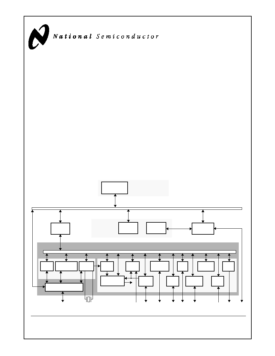
Block Diagram
Core Bus
Peripheral Bus
Bus
KBC + PM
Host I/F
RTC +
Processing
Unit
HBI
Host Bus
APC
Host
Config
RAM
Memory
External
BIU
CR16A Core
32.768
ICU
HFCG
PMC
ADC
KBSCAN
ACB
GPIO
WDG
Peripherals
Legacy
ROM
MIWU
IBM
®
, PC-AT
®
and PS/2
®
are registered trademarks of International Business Machines Corporation.
CompactRISC
TM
, WATCHDOG
TM
and TRI-STATE
®
are trademarks of National Semiconductor Corporation.
ACCESS.bus
®
is a registered trademark of Digital Equipment Corporation.
I
2
C
®
is a registered trademark of Philips.
Memory
(ISA Compatible)
MFT16
Timer +
KHz
Adapter
PS/2
I/F
I/F
CLK
DAC
+ I/O
(X2)

2
Highlights
www.national.com
Features
·
CR16A Core
-- 16-bit embedded RISC processor core
·
Bus Interface Unit (BIU)
-- Three address zones for static devices (SRAM,
ROM FLASH, I/O)
-- Configurable wait states and fast read bus cycles
·
Internal Memory
-- 2048 bytes of on-chip ROM
-- 1024 bytes of on-chip RAM
-- All memories can hold both code and data
·
External Memory
-- Supports BIOS memory (Flash) sharing with PC host
-- Up to 56 Kbyte for code and data
-- Field upgradable with Flash or SRAM devices
-- Supports host controlled code download and update
·
Host Bus Interface (HBI)
-- Three host interface channels, typically used for the
KBC, PM and RTC devices
-- Motherboard Plug and Play (PnP) configuration
o
With Enable and Lock bits for each device
o
Relocatable address for each device
-- Host power supply indicator input pin
-- 8042 KBC standard Interface (60h, 64h)
-- Intel 80C51SL compatible
-- IRQ1 and IRQ12 support
-- Fast Gate A20 and Fast host Reset, via firmware
-- PM interface port (62h, 66h)
-- PM port IRQ11
·
Real-Time Clock (RTC) and Advanced Power Control
(APC)
-- RTC
o
DS1287, MC146818 and PC87911 compatible
o
242 bytes battery backed-up CMOS RAM
o
Calendar including century and automatic leap-
year adjustment
o
Optional daylight saving adjustment
o
BCD or binary format for timekeeping
o
Three individually maskable interrupt event
flags: periodic rates from 122
µ
s to 500 ms; time-
of-day alarm, once per second to once per day
o
Separate backup battery pin
o
Double buffer time registers
o
The CMOS RAM and the RTC registers can be
accessed by the CR16A firmware
-- APC
o
Alarm wake-up
o
Hardware wake-up events
o
Software off events
·
HFCG
-- On-chip frequency multiplier
-- Single 32.786KHz crystal
-- Software controlled frequency generation
·
PMC
-- 3.3 and 5V operation with mixed voltage system
support
-- Reduced power consumption capability
-- Back-drive protection
-- Three power modes, switched by software or hard-
ware:
o
Active mode operating frequency 4-10MHz
o
Idle (20
µ
A)
o
Power Off - RTC only (0.9
µ
A typical) from back-
up battery
-- Automatic wake-up on system events
·
ICU
-- 16 maskable interrupt sources
-- Four general purpose external interrupt inputs
-- Programmable trigger mode (level: high or low,
edge: falling or rising)
-- Enable and pending indication for each interrupt
-- Non-maskable interrupt input
·
MIWU
-- Supports up to 24 wake-up or interrupt inputs
-- Generates wake-up to PMC
-- Generates interrupts to ICU
-- Provides user-selectable trigger conditions
·
GPIO
-- 76 ports
-- I/O pins individually configured as input or output
-- Configurable internal pull-up resistors
-- Special ports for internal keyboard matrix scanning
o
16 open-collector outputs
o
8 Schmidt inputs with internal pull-up
-- Special input for system On/Off switch
-- Supports very low-cost implementation of additional
off-chip I/O ports
·
PS/2 Interface
-- Supports three independent devices (external KBC,
mouse and additional pointing device)
-- Supports byte level handling via hardware accelerator
·
ACB Interface
-- Intel SMBus and Philips I
2
C
®
compatible
-- ACCESS.bus master and slave
-- Supports polling and interrupt controlled operation
-- Generates a wake-up signal on detection of a Start
Condition, while in power-down mode
-- Optional internal pull-up on SDA and SCL pins
3
Highlights
www.national.com
·
MFT16
-- Two 16-bit timers
-- Each timer supports Pulse Width Modulator (PWM),
Capture and Counter capabilities
·
TWD
-- 16-bit periodic interrupt timer with 30-
µ
s resolution
and 5-bit prescaler, for system tick and periodic
wake-up tasks
-- 8-bit WATCHDOG timer
·
ADC
-- Eight channels, 8-bit resolution
-- 10
µ
s conversion/channel
-- Internal or external voltage reference
·
DAC
-- Four channels, 8-bit resolution
-- 1
µ
s conversion time for 50 pF load
-- Full output range from AGND to AVCC
·
Supports Microsoft Advanced Power Management
(APM) specifications revision 1.2, February 1996
-- Generates the System Management Interrupt (SMI)
·
160-pin PQFP and 176-pin TQFP packages
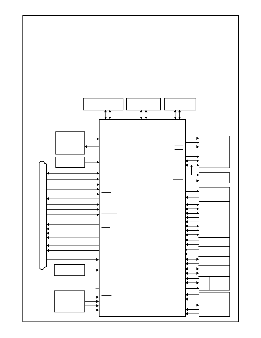
Basic Configuration
or
Clock
External
Memory
PC87570
Host System Bus (ISA Compatib
le)
32KX1/32KCLKIN
32KX2
HMR
HA18-0
HD7-0
HIOR
HIOW
IRQ1
IRQ11
IRQ12
RD
WR1-0
SEL0
A18-16, A15-0
D15-8
AD7-0
DA3-0
PA6-0
PB7-0
PC7-0
PD7-0
HIOCHRDY
RTC
Battery
V
BAT
IRQ8
PSCLK1
PSDAT1
Crystal
32.768 KHz
External Keyboard
Internal
Keyboard
KBSOUT15-0
KBSIN7-0
SRAM or
Flash
ENV0
GA20
AVCC
AGND
VCC
GND
Power
Supply
SCL
D7-0
HMEMRD
HMEMWR
PSCLK2
PSDAT2
PSCLK3
PSDAT3
PG4-0
PE1-0
PF7-0
PH5-0
HMEMCS
HAEN
EXINT0,10,11,15
PFAIL
RING
SHBM
HRMS
Configuration
Inputs
I/O
Expansion
TA
HDEN
TRIS
HPWRON
PC0
External Mouse
Auxiliary PS/2
Interface
Interface
Interface
HRSTO
SELIO
(Matrix)
SDA
TB
SWIN
Analog
Reset
Control
(power-up reset)
GPIO
Interrupt
ACCESS.bus
System
Timers
ENV1
NC
NC
SEL1
NC
(Application)
V
REF
ADC
DAC

4
Table of Contents
www.national.com
Table of Contents
Highlights
....................................................................................................................................................... 1
1.0
Introduction
1.1
INTERNAL ARCHITECTURE .................................................................................................... 14
1.1.1
Processing Unit ........................................................................................................... 14
1.1.2
BIU ............................................................................................................................... 14
1.1.3
Memory ........................................................................................................................ 14
1.1.4
HBI ............................................................................................................................... 14
1.1.5
Peripherals .................................................................................................................. 14
1.2
EXPANSION OPTIONS ............................................................................................................. 15
1.3
OPERATING ENVIRONMENTS ................................................................................................ 15
1.3.1
IRE Environment ......................................................................................................... 16
1.3.2
IRD Environment ......................................................................................................... 17
1.3.3
DEV Environment ........................................................................................................ 18
2.0
Signal/Pin Connection and Description
2.1
CONNECTION DIAGRAMS ...................................................................................................... 19
2.2
SIGNAL/PIN DESCRIPTIONS ................................................................................................... 21
2.3
RESET SOURCES AND TYPES ............................................................................................... 26
2.3.1
Power-Up Reset .......................................................................................................... 26
2.3.2
Warm Reset ................................................................................................................. 26
2.3.3
WATCHDOG Reset ..................................................................................................... 26
2.3.4
Triggering Reset .......................................................................................................... 26
2.4
STRAP PINS ............................................................................................................................ 26
2.4.1
Setting the Environment .............................................................................................. 26
2.4.2
Other Strap Pin Settings .............................................................................................. 26
2.4.3
System Load on Strap Pins ......................................................................................... 27
2.4.4
Strap Inputs During Idle Mode ..................................................................................... 27
2.4.5
Strap Pin Status Register (STRPST) ........................................................................... 27
2.5
ALTERNATE FUNCTIONS ........................................................................................................ 27
2.6
SYSTEM CONFIGURATION REGISTERS ............................................................................... 29
2.6.1
Module Configuration Register (MCFG) ...................................................................... 29
2.6.2
PAGE Register ............................................................................................................ 30
2.7
SHARED MEMORY CONFIGURATION ................................................................................... 30
2.8
MEMORY MAP .......................................................................................................................... 30
2.8.1
Accessing Base Memory ............................................................................................. 31
2.8.2
Accessing External Memory ........................................................................................ 32
2.8.3
Accessing I/O Expansion Space ................................................................................. 33
3.0
Bus Interface Unit (BIU)
3.1
FEATURES ................................................................................................................................ 34
3.2
FUNCTIONAL DESCRIPTION .................................................................................................. 34
3.2.1
Interfacing .................................................................................................................... 34
3.2.2
Static Memory and I/O Support ................................................................................... 34

5
Table of Contents
www.national.com
3.2.3
Byte Accessing ............................................................................................................ 34
3.3
CLOCK AND BUS CYCLES ...................................................................................................... 34
3.3.1
Clock Cycles ................................................................................................................ 34
3.3.2
Control Signals ............................................................................................................ 35
3.3.3
Early Write Bus Cycle .................................................................................................. 36
3.3.4
Late Write Bus Cycle ................................................................................................... 38
3.3.5
Normal Read Bus Cycle .............................................................................................. 40
3.3.6
Fast Read Bus Cycle ................................................................................................... 42
3.3.7
I/O Expansion Bus Cycles ........................................................................................... 43
3.3.8
I/O Expansion Example ............................................................................................... 44
3.4
DEVELOPMENT SUPPORT ..................................................................................................... 44
3.4.1
Bus Status Signals ...................................................................................................... 44
3.4.2
Core Bus Monitoring .................................................................................................... 44
3.5
BIU REGISTERS ....................................................................................................................... 45
3.5.1
BIU Configuration Register (BCFG) ............................................................................ 45
3.5.2
I/O Zone Configuration Register (IOCFG) ................................................................... 45
3.5.3
Static Zone Configuration Register (SZCFGn) ............................................................ 45
3.6
USAGE HINTS .......................................................................................................................... 46
4.0
On-Chip Memory
4.1
INTERNAL RAM ........................................................................................................................ 47
4.2
INTERNAL ROM ........................................................................................................................ 47
4.2.1
Access Times .............................................................................................................. 47
4.2.2
ROM Shadow .............................................................................................................. 47
5.0
Host Bus Interface (HBI)
5.1
FEATURES ................................................................................................................................ 48
5.2
HOST ACCESS TO SHARED MEMORY DEVICE ................................................................... 49
5.2.1
Enabling Shared Memory Mode .................................................................................. 49
5.2.2
Memory Device Interface ............................................................................................. 49
5.2.3
Host Access to Shared Memory .................................................................................. 49
5.3
CORE ACCESS TO RTC/APC .................................................................................................. 49
5.3.1
Host and CR16A Arbitration over RTC/APC ............................................................... 49
5.4
USAGE HINTS .......................................................................................................................... 49
5.4.1
Shared Memory ........................................................................................................... 49
5.4.2
Wake-Up from Host ..................................................................................................... 50
5.4.3
Host Power-on Indication ............................................................................................ 50
5.5
HOST ACCESS TO PC87570 RESIDENT I/O DEVICES ......................................................... 50
5.5.1
Host Access to Configuration Registers ...................................................................... 50
5.5.2
Host Access to Resident I/O Devices .......................................................................... 50
5.5.3
Host Bus I/O Cycles .................................................................................................... 50
5.6
KBC CHANNEL ......................................................................................................................... 50
5.6.1
Status Register ............................................................................................................ 50
5.6.2
DBBOUT Register ....................................................................................................... 51
5.6.3
DBBIN Register ........................................................................................................... 51