
PC87351 PC98 and ACPI Compliant SuperI/O with System Wake-Up Control
www.national.com
PRELIMINARY
May 1998
PC87351 PC98 and ACPI Compliant SuperI/O with
System Wake-Up Control
Highlights
General Description
The PC87351, a member of National Semiconductor's Su-
perI/O family of integrated PC peripherals, is a 128-pin,
PC98 and ACPI compliant SuperI/O that offers a single-chip
solution to the most commonly used ISA peripherals.
The PC87351 incorporates: a Floppy Disk Controller (FDC)
which is available also on the Parallel Port pins as a multi-
plexed option (PPM), two enhanced Serial Ports, Infrared
Comunication Port (HP-SIR, Sharp-IR, and Consumer
Electronics-IR), a full IEEE 1284 Parallel Port, a Keyboard
and Mouse Controller (KBC), System Wake-Up Control
(SWC), General-Purpose Input/Output (GPIO) Ports with
assert interrupt capability, and Fan Speed Control (FSC).
Outstanding Features
·
Fan Speed Control for two fans
·
11 General-Purpose I/O Ports, bi-directional, with in-
terrupt assertion capability
·
System Wake-Up Control powered by V
SB
, generates
power-up request in response to preprogrammed key-
board or mouse sequence, modem, telephone ring,
and two general-purpose events without an external
clock
·
Serial or parallel IRQ support
·
Programmable write protect for Floppy Disk Controller
·
Power-fail recovery support
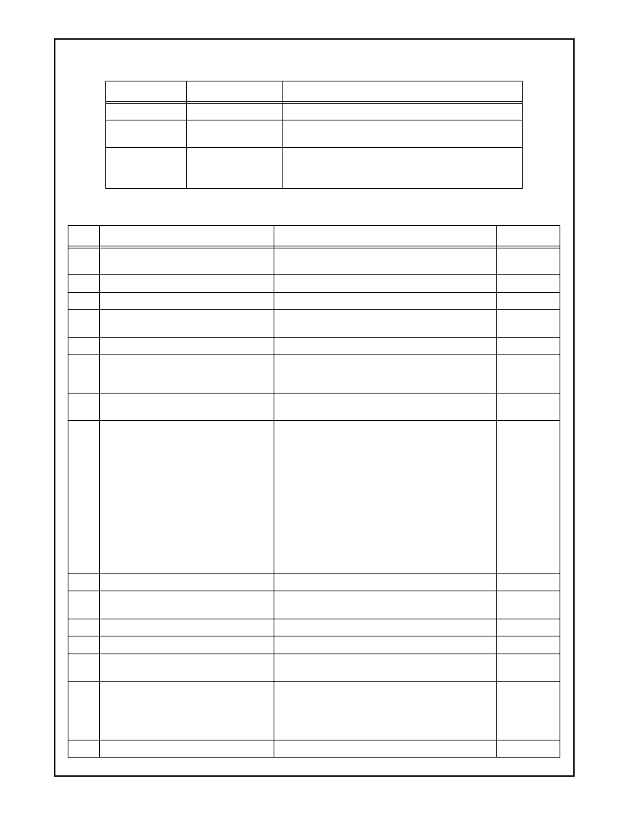
Block Diagram
Controller
System Wake-Up
IEEE 1284
Wake-Up
Parallel Port
Ports
Keyboard and Mouse
Interface
Floppy Disk
Controller
Keyboard and Mouse
Control
Events
Host Interface
ISA
Interface SERIRQ
I/O Ports
General-Purpose
I/O
PWUREQ
Serial Port 2
Serial
Infrared
Interface Interface
Serial Port 1
Serial
Interface
V
SB
V
BAT
FANOUT0 FANOUT1
Fan Speed Control
with IR
Floppy Drive
Interface
Interface
Parallel Port/
Floppy Drive
PPM
IBM
®
, MicroChannel
®
, PC-AT
®
and PS/2
®
are registered trademarks of International Business Machines Corporation.
Microsoft
®
and Windows
®
are registered trademarks of Microsoft Corporation.
TRI-STATE
®
is a registered trademark of National Semiconductor Corporation.
©
1998 National Semiconductor Corporation

2
Highlights
(Continued)
www.national.com
Features
·
PC98 and ACPI Compliant
-- PnP Configuration Register structure
-- Flexible resource allocation for all logical devices
t
Relocatable base address
t
9 Parallel IRQ or 15 Serial IRQ routing options
t
3 optional 8-bit DMA channels (where applica-
ble)
·
Floppy Disk Controller (FDC)
-- Software compatible with the PC8477, which con-
tains a superset of the FDC functions in the
µ
DP8473, the NEC
µ
PD765A and the N82077
-- 16-byte FIFO
-- Burst and non-burst modes
-- High-performance, digital data separator that does
not require any external filter components
-- Standard 5.25" and 3.5" Floppy Disk Drive (FDD)
support
-- Perpendicular recording drive support
-- Three-mode FDD support
-- Full support for IBM Tape Drive Register (TDR) im-
plementation of AT and PS/2 drive types
-- Programmable write protect
·
Parallel Port
-- Software or hardware control
-- Enhanced Parallel Port (EPP) compatible with new
version EPP 1.9 and IEEE 1284 compliant
-- EPP support for version EPP 1.7 of the Xircom spec-
ification
-- EPP support as mode 4 of the Extended Capabilities
Port (ECP)
-- IEEE 1284 compliant ECP, including level 2
-- Selection of internal pull-up or pull-down resistor for
Paper End (PE) pin
-- PCI bus utilization reduction by supporting a de-
mand DMA mode mechanism and a DMA fairness
mechanism
-- Protection circuit that prevents damage to the paral-
lel port when a printer connected to it powers up or
is operated at high voltages, even if the device is in
power-down
-- Output buffers that can sink and source 14 mA
·
Parallel Port Multiplexer (PPM)
-- Additional set of FDC signals multiplexed on Parallel
Port pins
-- Optional connection of additional, external FDD on
Parallel Port connector
·
Serial Port 1
-- Software compatible with the 16550A and the 16450
-- Shadow register support for write-only bit monitoring
-- UART data rates up to 1.5 Mbaud
·
Serial Port 2 with Infrared
-- Software compatible with the 16550A and the 16450
-- Shadow register support for write-only bit monitoring
-- UART data rates up to 1.5 Mbaud
-- HP-SIR
-- ASK-IR option of SHARP-IR
-- DASK-IR option of SHARP-IR
-- Consumer Remote Control supports RC-5, RC-6,
NEC, RCA and RECS 80
-- Non-standard DMA support
-
1 or 2 channels
·
Keyboard and Mouse Controller (KBC)
-- 8-bit microcontroller
-- Software compatible with the 8042AH and PC87911
microcontrollers
-- 2 KB custom-designed program ROM
-- 256 bytes RAM for data
-- Four programmable dedicated open-drain I/O lines
-- Asynchronous access to two data registers and one
status register during normal operation
-- Support for both interrupt and polling
-- 93 instructions
-- 8-bit timer/counter
-- Support for binary and BCD arithmetic
-- Operation at 8 MHz,12 MHz or 16 MHz (programma-
ble option)
-- Can be customized by using the PC87323, which in-
cludes a RAM-based KBC as a development plat-
form for KBC code
·
11 General-Purpose Bi-Directional I/O (GPIO) Ports
-- 11 GPIO pins with interrupt assertion capability
-- Programmable drive type for each output pin (open-
drain, push-pull or output disable)
-- Programmable option for internal pull-up resistor on
each input pin
-- Output lock option
-- Back-drive protection circuit
·
System Wake-Up Control (SWC)
-- Power-up request upon detection of Keyboard,
Mouse, RI1, RI2, RING, PME1 and PME2 activity, as
follows:
t
Preprogrammed Keyboard or Mouse sequence
t
External modem ring on serial ports
t
Ring pulse or pulse train on the RING input
t
General purpose events, PME1 and PME2
-- Optional routing of power-up request on IRQ line
-- Powered by V
SB
-- Battery-backed wake-up setup
-- Power-fail recovery support
4
www.national.com
Datasheet Revision Record
Revision Date
Status
Comments
January 1998
Advanced Information First pass with pin assignment
March 1998
Preliminary
Implemented:
Item 1, Important Notice, pin reassignment
May 1998
Preliminary
Implemented:
Items 2-31 below
Paginated Datasheet Revision Record in datasheet body
Item
Topic
Change/Correction
Location
2
Pin description
Table describing KBCLK, KBDAT, MCLK and MDAT
signals enhanced to identify pin drivers
Section 1.4.7
3
PPM power save mode
All references deleted
Chapter 2
4
Device architecture
9 logical devices
Section 2.1
5
Index 74h, 75h
DMA Channel Select 0, 1
Modified
Section 2.2.3,
Table 2-7
6
VSB Power-Up Reset
Hardware reset explanation modified
Section 2.2.5
7
New section added
REGISTER TYPE ABBREVIATIONS added before
the existing section; all subsequent numbering
changed
Section 2.3
8
SuperI/O Configuration 1 Register
Bit 3
Reserved
Section 2.4.3
9
SuperI/O Configuration 2 Register
Bits
6 5
Function
0 0
GPIO17
0 1
KBRST (default)
1 0
P12
1 1
PNF (PPM mode enabled)
Bits
2 1 0
Function
0 0 X
GPIO14 (default)
0 1 1
GPIO14
0 1 0
IRQ9
1 0 X
IRRX2/IRSL0
1 1 X
P17
Section 2.4.4
10
SuperI/O Revision ID Register
Location and Type added
Section 2.4.7
11
Keyboard and Mouse Controller
All references to TEST0 and TEST1 changed to T0
and T1, respectively.
Section 2.11.1
12
Implementation
Ports 1 and 2 description deleted
Section 2.12.2
13
GPIO Configuration Registers' Access
Drawing modified
Figure 2-6
14
GPIO Pin Configuration Select Register
Bits 5-4
01, 10: Binary value of the port number, 1-2 respectively
11: Reserved
Section 2.12.4
15
Fan Speed Control
General Description modified; nomenclature of Fan
Control Duty Cycle and Fan Control Pre-Scale
registers changed; references to Fan Speed Monitor
deleted; configuration parameters (Reset and Type)
modified
Section 2.13
16
System events
Number of events changed to seven
Section 3.2
Datasheet Revision Record
(Continued)
5
www.national.com
17
Keyboard Data Shift Register
Description modified
Section 3.4.6
18
Mouse Data Shift Register
Description modified
Section 3.4.7
19
Ports with fewer than 8 bits
Implementation description
Chapter 4
20
Interrupt Assertion and Handling
Bit nomenclature modified
Section 4.3
21
GPIO Pin Configuration Access Register Bit nomenclature and descriptions changed
Section 4.4.1
22
GPIO Data Out Register
Bitmap and Reset values added
Section 4.4.3
23
GPIO Data In Register
Bitmap and Reset values added
Section 4.4.4
24
GPIO Interrupt Enable Register
Bitmap and Reset values added
Section 4.4.5
25
GPIO Status Register
Bitmap and Reset values added
Section 4.4.6
26
Functional Description
Corrected and enhanced
Section 5.2
27
Fan Control Duty Cycle Register
Bits 7-0
00h: PWM output is continuously low
01h-FEh: PWM output is high for [Duty Cycle Value] clock
cycles and low for [256-Duty Cycle Value] clock cycles
FFh: PWM output is continuously high
Section 5.3.3
28
Device Specifications
Timing diagrams drawn more precisely
Chapter 11
29
V
BAT
Battery Supply Current
Conditions and Max modified
Section 11.1.4
30
Host Interface I/O Cycle Timing
t
RDYA
, t
RDYl
and t
RWl
added to table; footnote 2 added
to table; IOCHRDY timing diagram added
Section 11.2.3
31
Serial IRQ Timing
Output timing diagram modified
Section 11.2.6
Item
Topic
Change/Correction
Location
