TL F 5165
MM54HC245AMM74HC245A
Octal
TRI-STATE
Transceiver
January 1988
MM54HC245A MM74HC245A
Octal TRI-STATE
Transceiver
General Description
This TRI-STATE bidirectional buffer utilizes advanced sili-
con-gate CMOS technology and is intended for two-way
asynchronous communication between data buses It has
high drive current outputs which enable high speed opera-
tion even when driving large bus capacitances This circuit
possesses the low power consumption and high noise im-
munity usually associated with CMOS circuitry yet has
speeds comparable to low power Schottky TTL circuits
This device has an active low enable input G and a direction
control input DIR When DIR is high data flows from the A
inputs to the B outputs When DIR is low data flows from
the B inputs to the A outputs
The MM54HC245A
MM74HC245A transfers true data from one bus to the oth-
er
This device can drive up to 15 LS-TTL Loads and does not
have Schmitt trigger inputs All inputs are protected from
damage due to static discharge by diodes to V
CC
and
ground
Features
Y
Typical propagation delay 13 ns
Y
Wide power supply range 2 Ł 6V
Y
Low quiescent current 80 mA maximum (74 HC)
Y
TRI-STATE outputs for connection to bus oriented
systems
Y
High output drive 6 mA (minimum)
Y
Same as the '645
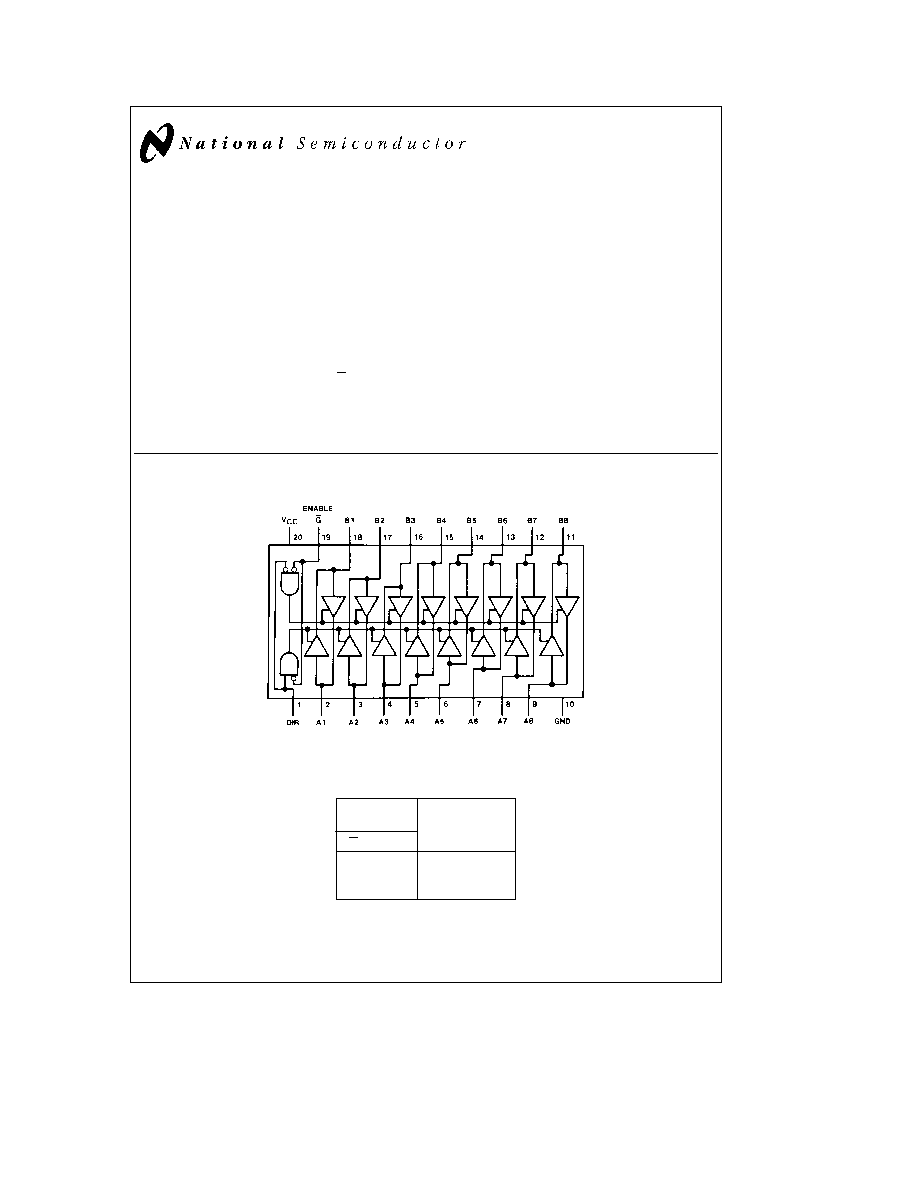
Connection Diagram
Dual-In-Line Package
TL F 5165 Ł 1
Top View
Order Number MM54HC245A or MM74HC245A
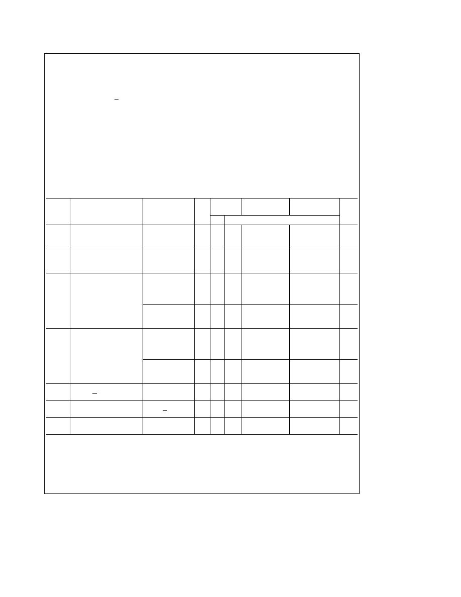
Truth Table
Control
Inputs
Operation
G
DIR
L
L
B data to A bus
L
H
A data to B bus
H
X
Isolation
H
e
high level L
e
low level X
e
irrelevant
TRI-STATE
is a registered trademark of National Semiconductor Corp
C1995 National Semiconductor Corporation
RRD-B30M105 Printed in U S A
Absolute Maximum Ratings
(Notes 1
2)
If Military Aerospace specified devices are required
please contact the National Semiconductor Sales
Office Distributors for availability and specifications
Supply Voltage (V
CC
)
b
0 5 to
a
7 0V
DC Input Voltage DIR and G pins (V
IN
)
b
1 5 to V
CC
a
1 5V
DC Input Output Voltage (V
IN
V
OUT
)
b
0 5 to V
CC
a
0 5V
Clamp Diode Current (I
CD
)
g
20 mA
DC Output Current per pin (I
OUT
)
g
35 mA
DC V
CC
or GND Current per pin (I
CC
)
g
70 mA
Storage Temperature Range (T
STG
)
b
65 C to
a
150 C
Power Dissipation (P
D
)
(Note 3)
600 mW
S O Package only
500 mW
Lead Temp (T
L
) (Soldering 10 seconds)
260 C
Operating Conditions
Min
Max
Units
Supply Voltage (V
CC
)
2
6
V
DC Input or Output Voltage
(V
IN
V
OUT
)
0
V
CC
V
Operating Temp Range (T
A
)
MM74HC
b
40
a
85
C
MM54HC
b
55
a
125
C
Input Rise Fall Times
(t
r
t
f
)
V
CC
e
2 0V
1000
ns
V
CC
e
4 5V
500
ns
V
CC
e
6 0V
400
ns
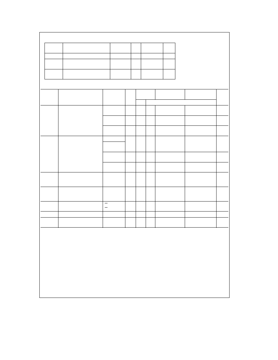
DC Electrical Characteristics
(Note 4)
T
A
e
25 C
74HC
54HC
Symbol
Parameter
Conditions
V
CC
T
A
e b
40 to 85 C
T
A
e b
55 to 125 C
Units
Typ
Guaranteed Limits
V
IH
Minimum High Level Input
2 0V
1 5
1 5
1 5
V
Voltage
4 5V
3 15
3 15
3 15
V
6 0V
4 2
4 2
4 2
V
V
IL
Maximum Low Level Input
2 0V
0 5
0 5
0 5
V
Voltage
4 5V
1 35
1 35
1 35
V
6 0V
1 8
1 8
1 8
V
V
OH
Minimum High Level Output
V
IN
e
V
IH
or V
IL
Voltage
l
I
OUT
l
s
20 mA
2 0V
2 0
1 9
1 9
1 9
V
4 5V
4 5
4 4
4 4
4 4
V
6 0V
6 0
5 9
5 9
5 9
V
V
IN
e
V
IH
or V
IL
l
I
OUT
l
s
6 0 mA
4 5V
4 2
3 98
3 84
3 7
V
l
I
OUT
l
s
7 8 mA
6 0V
5 7
5 48
5 34
5 2
V
V
OL
Maximum Low Level Output
V
IN
e
V
IH
or V
IL
Voltage
l
I
OUT
l
s
20 mA
2 0V
0
0 1
0 1
0 1
V
4 5V
0
0 1
0 1
0 1
V
6 0V
0
0 1
0 1
0 1
V
V
IN
e
V
IH
or V
IL
l
I
OUT
l
s
6 0 mA
4 5V
0 2
0 26
0 33
0 4
V
l
I
OUT
l
s
7 8 mA
6 0V
0 2
0 26
0 33
0 4
V
I
IN
Input Leakage
V
IN
e
V
CC
to GND
6 0V
g
0 1
g
1 0
g
1 0
m
A
Current (G and DIR)
I
OZ
Maximum TRI-STATE Output
V
OUT
e
V
CC
or GND
6 0V
g
0 5
g
5 0
g
10
m
A
Leakage Current
Enable G
e
V
IH
I
CC
Maximum Quiescent Supply
V
IN
e
V
CC
or GND
6 0V
8 0
80
160
m
A
Current
I
OUT
e
0 mA
Note 1
Maximum Ratings are those values beyond which damage to the device may occur
Note 2
Unless otherwise specified all voltages are referenced to ground
Note 3
Power Dissipation temperature derating
plastic ``N'' package
b
12 mW C from 65 C to 85 C ceramic ``J'' package
b
12 mW C from 100 C to 125 C
Note 4
For a power supply of 5V
g
10% the worst case output voltages (V
OH
and V
OL
) occur for HC at 4 5V Thus the 4 5V values should be used when designing
with this supply Worst case V
IH
and V
IL
occur at V
CC
e
5 5V and 4 5V respectively (The V
IH
value at 5 5V is 3 85V ) The worst case leakage current (I
IN
I
CC
and
I
OZ
) occur for CMOS at the higher voltage and so the 6 0V values should be used
V
IL
limits are currently tested at 20% of V
CC
The above V
IL
specification (30%) of V
CC
) will be implemented no later than Q1 CY'89 O
e
V
IL
2
AC Electrical Characteristics
V
CC
e
5V T
A
e
25 C t
r
e
t
f
e
6 ns
Symbol
Parameter
Conditions
Typ
Guaranteed
Units
Limit
t
PHL
t
PLH
Maximum Propagation Delay
C
L
e
45 pF
12
17
ns
t
PZH
t
PZL
Maximum Output Enable Time
R
L
e
1 kX
24
35
ns
C
L
e
45 pF
t
PHZ
t
PLZ
Maximum Output Disable Time
R
L
e
1 kX
18
25
ns
C
L
e
5 pF
AC Electrical Characteristics
V
CC
e
2 0V to 6 0V C
L
e
50 pF t
r
e
t
f
e
6 ns (unless otherwise specified)
T
A
e
25 C
74HC
54HC
Symbol
Parameter
Conditions
V
CC
T
A
e b
40 to 85 C
T
A
e b
55 to 125 C
Units
Typ
Guaranteed Limits
t
PHL
Maximum Propagation Delay
C
L
e
50 pF
2 0V
31
90
113
135
ns
t
PLH
C
L
e
150 pF
2 0V
41
96
116
128
ns
C
L
e
50 pF
4 5V
13
18
23
27
ns
C
L
e
150 pF
4 5V
17
22
28
33
ns
C
L
e
50 pF
6 0V
11
15
19
23
ns
C
L
e
150 pF
6 0V
14
19
23
28
ns
t
PZH
Maximum Output Enable
R
L
e
1 kX
t
PZL
Time
C
L
e
50 pF
2 0V
71
190
240
285
ns
C
L
e
150 pF
2 0V
81
240
300
360
ns
C
L
e
50 pF
4 5V
26
38
48
57
ns
C
L
e
150 pF
4 5V
31
48
60
72
ns
C
L
e
50 pF
6 0V
21
32
41
48
ns
C
L
e
150 pF
6 0V
25
41
51
61
ns
t
PHZ
Maximum Output Disable
R
L
e
1 kX
2 0V
39
135
169
203
ns
t
PLZ
Time
C
L
e
50 pF
4 5V
20
27
34
41
ns
6 0V
18
23
29
34
ns
t
TLH
t
THL
Output Rise and Fall Time
C
L
e
50 pF
2 0V
20
60
75
90
ns
4 5V
6
12
15
18
ns
6 0V
5
10
13
15
ns
C
PD
Power Dissipation
G
e
V
IL
50
pF
Capacitance (Note 5)
G
e
V
IH
5
pF
C
IN
Maximum Input Capacitance
5
10
10
10
pF
C
IN OUT
Maximum Input Output
15
20
20
20
pF
Capacitance A or B
Note 5
C
PD
determines the no load dynamic power consumption P
D
e
C
PD
V
CC
2
f
a
I
CC
V
CC
and the no load dynamic current consumption I
S
e
C
PD
V
CC
f
a
I
CC
3
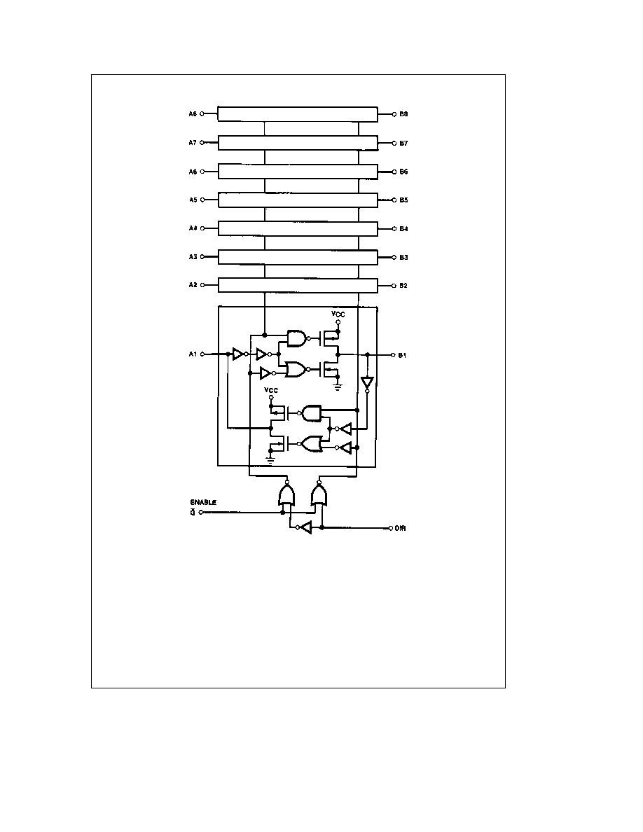
Logic Diagram
TL F 5165 Ł 2
4
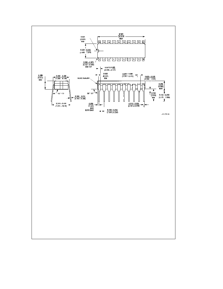
Physical Dimensions
inches (millimeters)
Order Number MM54HC245A or MM74HC245A
NS Package J20A
5