
TL F 5889
MM54C90MM74C90
4-Bit
Decade
Counter
MM54C93MM74C93
4-Bit
Binary
Counter
February 1988
MM54C90 MM74C90 4-Bit Decade Counter
MM54C93 MM74C93 4-Bit Binary Counter
General Description
The
MM54C90 MM74C90
decade
counter
and
the
MM54C93 MM74C93 binary counter and complementary
MOS (CMOS) integrated circuits constructed with N- and
P-channel enhancement mode transistors The 4-bit decade
counter can reset to zero or preset to nine by applying ap-
propriate logic level on the R
01
R
02
R
91
and R
92
inputs
Also a separate flip-flop on the A-bit enables the user to
operate it as a divide-by-2 5 or 10 frequency counter The
4-bit binary counter can be reset to zero by applying high
logic level on inputs R
01
and R
02
and a separate flip-flop on
the A-bit enables the user to operate it as a divide-by-2 -8
or -16 divider Counting occurs on the negative going edge
of the input pulse
All inputs are protected against static discharge damage
Features
Y
Wide supply voltage range
3V to 15V
Y
Guaranteed noise margin
1V
Y
High noise immunity
0 45 V
CC
(typ )
Y
Low power
Fan out of 2
TTL compatiblity
driving 74L
Y
The
MM54C93 MM74C93
follows
the
MM54L93
MM74L93 Pinout
Connection and Logic Diagrams
MM54C90 MM74C90
Dual-In-Line Package
TL F 5889 � 2
Top View
MM54C93 MM74C93
Dual-In-Line Package
TL F 5889 � 4
Top View
Order Number MM54C90 or MM74C93
M54C90 MM74C90
TL F 5889 � 1
MM54C93 MM74C93
TL F 5889 � 3
C1995 National Semiconductor Corporation
RRD-B30M105 Printed in U S A

Absolute Maximum Ratings
If Military Aerospace specified devices are required
please contact the National Semiconductor Sales
Office Distributors for availability and specifications
Voltage at Any Pin (Note 1)
b
0 3V to V
CC
a
0 3V
Operating Temperature Range (T
A
)
MM54C90 MM54C93
b
55 C to
a
125 C
MM74C90 MM74C93
b
40 C to
a
85 C
Power Dissipation (P
D
)
Dual-In-Line
700 mW
Small Outline
500 mW
Operating V
CC
Range
3V to 15V
Absolute Maximum V
CC
18V
Storage Temperature Range (T
S
)
b
65 C to
a
150 C
Lead Temperature (T
L
)
(Soldering 10 seconds)
260 C
DC Electrical Characteristics
Min Max limits apply across temperature range unless otherwise noted
Symbol
Parameter
Conditions
Min
Typ
Max
Units
CMOS TO CMOS
V
IN(1)
Logical ``1'' Input Voltage
V
CC
e
5V
3 5
V
V
CC
e
10V
8 0
V
V
IN(0)
Logical ``0'' Input Voltage
V
CC
e
5V
1 5
V
V
CC
e
10V
2 0
V
V
OUT(1)
Logical ``1'' Output Voltage
V
CC
e
5V I
O
e b
10 mA
4 5
V
V
CC
e
10V I
O
e b
10 mA
9 0
V
V
OUT(0)
Logical ``0'' Output Voltage
V
CC
e
5V I
O
e a
10 mA
0 5
V
V
CC
e
10V I
O
e a
10 mA
1 0
V
I
IN(1)
Logical ``1'' Input Current
V
CC
e
15V V
IN
e
15V
0 005
1 0
m
A
I
IN(0)
Logical ``0'' Input Current
V
CC
e
15V V
IN
e
0V
b
1 0
b
0 005
m
A
I
CC
Supply Current
V
CC
e
15V
0 05
300
m
A
CMOS LPTTL INTERFACE
V
IN(1)
Logical ``1'' Input Voltage
MM54C90 MM54C93
V
CC
e
4 5V
V
CC
b
1 5
V
MM74C90 MM74C93
V
CC
e
4 75V
V
CC
b
1 5
V
V
IN(0)
Logical ``0'' Input Voltage
MM54C90 MM54C93
V
CC
e
4 5V
0 8
V
MM74C90 MM74C93
V
CC
e
4 75V
0 8
V
V
OUT(1)
Logical ``1'' Output Voltage
MM54C90 MM54C93
V
CC
e
4 5V I
O
e b
360 mA
2 4
V
MM74C90 MM74C93
V
CC
e
4 75V I
O
e b
360 mA
2 4
V
V
OUT(0)
Logical ``0'' Output Voltage
MM54C90 MM54C93
V
CC
e
4 5V I
O
e b
360 mA
0 4
V
MM74C90 MM74C93
V
CC
e
4 75V I
O
e b
360 mA
0 4
V
OUTPUT DRIVE (See 54C 74C Family Characteristics Data Sheet) (Short Circuit Current)
I
SOURCE
Output Source Current
V
CC
e
5V V
OUT
e
0V
b
1 75
b
3 3
mA
(P-Channel)
T
A
e
25 C
I
SOURCE
Output Source Current
V
CC
e
10V V
OUT
e
0V
b
8 0
b
15
mA
(P-Channel)
T
A
e
25 C
I
SINK
Output Sink Current
V
CC
e
5V V
OUT
e
V
CC
1 75
3 6
mA
(N-Channel)
T
A
e
25 C
I
SINK
Output Sink Current
V
CC
e
10V V
OUT
e
V
CC
8 0
16
mA
(N-Channel)
T
A
e
25 C
Note 1
``Absolute Maximum Ratings'' are those values beyond which the safety of the device cannot be guaranteed Except for ``Operating Temperature Range''
they are not meant to imply that the devices should be operated at these limits The table of ``Electrical Characteristics'' provides conditions for actual device
operation
AC Electrical Characteristics
T
A
e
25 C C
L
e
50 pF unless otherwise specified
Symbol
Parameter
Conditions
Min
Typ
Max
Units
t
pd0
t
pd1
Propagation Delay Time
V
CC
e
5V
200
400
ns
from A
IN
to Q
A
V
CC
e
10
80
150
ns
t
pd0
t
pd1
Propagation Delay Time from
V
CC
e
5V
450
850
ns
A
IN
to Q
B
(MM54C93 MM74C93)
V
CC
e
10V
160
300
ns
t
pd0
t
pd1
Propagation Delay Time from
V
CC
e
5V
450
800
ns
A
IN
to Q
B
(MM54C90 MM74C90)
V
CC
e
10V
160
300
ns
2
AC Electrical Characteristics
T
A
e
25 C C
L
e
50 pF unless otherwise specified (Continued)
Symbol
Parameter
Conditions
Min
Typ
Max
Units
t
pd0
t
pd1
Propagation Delay Time
V
CC
e
5V
500
1050
ns
from A
IN
to Q
C
(MM54C93 MM74C93)
V
CC
e
10
200
400
ns
t
pd0
t
pd1
Propagation Delay Time from
V
CC
e
5V
500
1000
ns
A
IN
to Q
C
(MM54C93 MM74C93)
V
CC
e
10V
200
400
ns
t
pd0
t
pd1
Propagation Delay Time from
V
CC
e
5V
600
1200
ns
A
IN
to Q
D
(MM54C93 MM74C93)
V
CC
e
10V
250
500
ns
t
pd0
t
pd1
Propagation Delay Time from
V
CC
e
5V
450
800
ns
A
IN
to Q
D
(MM54C90 MM74C90)
V
CC
e
10V
160
300
ns
t
pd0
t
pd1
Propagation Delay Time from
V
CC
e
5V
150
300
ns
R
01
or R
02
to Q
A
Q
B
Q
C
or Q
D
V
CC
e
10V
75
150
ns
(MM54C93 MM74C93)
t
pd0
t
pd1
Propagation Delay Time from
V
CC
e
5V
200
400
ns
R
01
or R
02
to Q
A
Q
B
Q
C
or Q
D
V
CC
e
10V
75
150
ns
(MM54C90 MM74C90)
t
pd0
t
pd1
Propagation Delay Time from
V
CC
e
5V
250
500
ns
R
91
or R
92
to Q
A
or Q
D
V
CC
e
10V
100
200
ns
(MM54C90 MM74C90)
t
PW
Min R
01
or R
02
Pulse Width
V
CC
e
5V
600
250
ns
(MM54C93 MM74C93)
V
CC
e
10V
30
125
ns
t
PW
Min R
01
or R
02
Pulse Width
V
CC
e
5V
600
250
ns
(MM54C90 MM74C90)
V
CC
e
10V
300
125
ns
t
PW
Min R
91
or R
92
Pulse Width
V
CC
e
5V
500
200
ns
(MM54C90 MM74C90)
V
CC
e
10V
250
100
ns
t
r
t
f
Maximum Clock Rise
V
CC
e
10V
15
m
s
and Fall Time
V
CC
e
10V
5
m
s
t
W
Minimum Clock Pulse Width
V
CC
e
5V
250
100
ns
V
CC
e
10V
100
50
ns
f
MAX
Maximum Clock Frequency
V
CC
e
5V
2
MHz
V
CC
e
10V
5
MHz
C
IN
Input Capacitance
Any Input (Note 2)
5
pF
C
PD
Power Dissipation Capacitance
Per Package (Note 3)
45
pF
AC Parameters are guaranteed by DC correlated testing
Note 1
``Absolute Maximum Ratings'' are those values beyond which the safety of the device cannot be guaranteed Except for ``Operating Temperature Range''
they are not meant to imply that the devices should be operated at these limits The table of ``Electrical Characteristics'' provides conditions for actual device
operation
Note 2
Capacitance is guaranteed by periodic testing
Note 3
C
PD
determines the no load ac power consumption of any CMOS device For complete explanation see 54C 74C Family Characteristics application note
AN-90
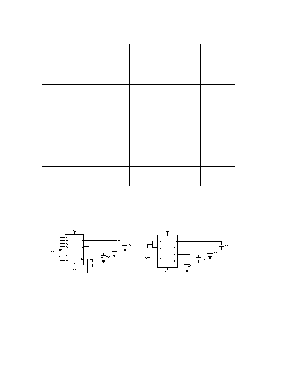
AC Test Circuits
MM54C90 MM74C90
TL F 5889 � 5
Clock rise and fall time t
r
e
t
f
e
20 ns
MM54C93 MM74C93
TL F 5889 � 6
Clock rise and fall time t
r
e
t
f
e
20 ns
3

Switching Time Waveforms
TL F 5889 � 7
Note 1
MM54C90 MM74C90 and MM54C93
MM74C93 are solid line waveforms Dashed line
waveforms are for MM54C90 MM74C90 only
Truth Table
MM54C90 MM74C90 4-Bit Decade Counter
BCD Count Sequence
Count
Output
Q
D
Q
C
Q
B
Q
A
0
L
L
L
L
1
L
L
L
H
2
L
L
H
L
3
L
L
H
H
4
L
H
L
L
5
L
H
L
H
6
L
H
H
L
7
L
H
H
H
8
H
L
L
L
9
H
L
L
H
Output Q
A
is connected to Input B for
BCD count
H
e
High Level
L
e
Low Level
X
e
Irrelevant
Reset Count Function Table
Reset Inputs
Output
R
01
R
02
R
91
R
92
Q
D
Q
C
Q
B
Q
A
H
H
L
X
L
L
L
L
H
H
X
L
L
L
L
L
X
X
H
H
H
L
L
H
X
L
X
L
Count
L
X
L
X
Count
L
X
X
L
Count
X
L
L
X
Count
MM54C93 MM74C93 4-Bit Binary Counter
Binary Count Sequence
Count
Output
Q
D
Q
C
Q
B
Q
A
0
L
L
L
L
1
L
L
L
H
2
L
L
H
L
3
L
L
H
H
4
L
H
L
L
5
L
H
L
H
6
L
H
H
L
7
L
H
H
H
8
H
L
L
L
9
H
L
L
H
10
H
L
H
L
11
H
L
H
H
12
H
H
L
L
13
H
H
L
H
14
H
H
H
L
15
H
H
H
H
Output Q
A
is connected to input B for
binary count sequence
H
e
High Level
L
e
Low Level
X
e
Irrelevant
Reset Count Function Table
Reset
Output
Inputs
R
01
R
02
Q
D
Q
C
Q
B
Q
A
H
H
L
L
L
L
L
X
Count
X
L
Count
4

Physical Dimensions
inches (millimeters)
Ceramic Dual-In-Line Package (J)
Order Number MM54C90J MM54C93J MM74C90J or MM74C93J
NS Package Number J14A
5