TL F 5899
MM54C174MM74C174
Hex
D
Flip-Flop
February 1988
MM54C174 MM74C174 Hex D Flip-Flop
General Description
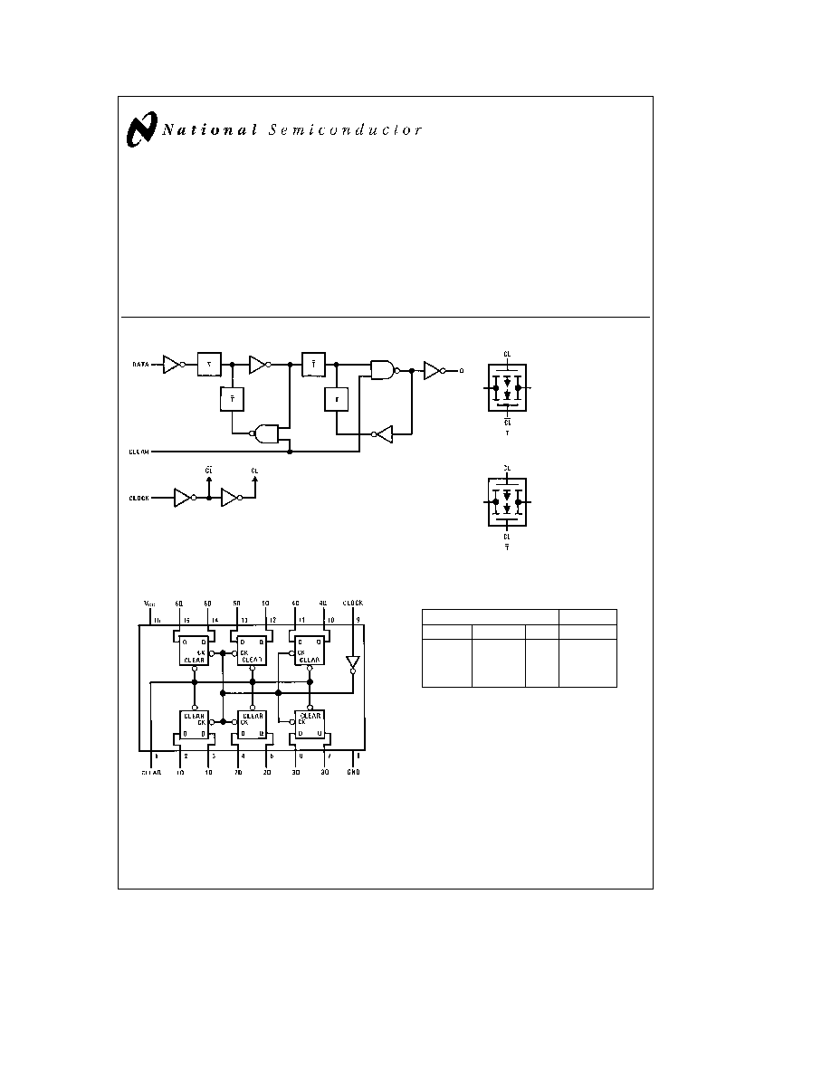
The MM54C174 MM74C174 hex D flip-flop is a monolithic
complementary MOS (CMOS) integrated circuit constructed
with N- and P-channel enhancement transistors All have a
direct clear input Information at the D inputs meeting the
setup time requirements is transferred to the Q outputs on
the positive-going edge of the clock pulse Clear is indepen-
dent of clock and accomplished by a low level at the clear
input All inputs are protected by diodes to V
CC
and GND
Features
Y
Wide supply voltage range
3 0V to 15V
Y
Guaranteed noise margin
1 0V
Y
High noise immunity
0 45 V
CC
(typ )
Y
Low power TTL compatibility
Fan out of 2
driving 74L
Logic and Connection Diagrams
TL F 5899 � 1
TL F 5899 � 2
TL F 5899 � 3
Dual-In-Line Package
TL F 5899 � 4
Top View
Order Number MM54C174 or MM74C174
Truth Table
Inputs
Output
Clear
Clock
D
Q
L
X
X
L
H
u
H
H
H
u
L
L
H
L
X
Q
C1995 National Semiconductor Corporation
RRD-B30M105 Printed in U S A
Absolute Maximum Ratings
(Note 1)
If Military Aerospace specified devices are required
please contact the National Semiconductor Sales
Office Distributors for availability and specifications
Voltage at Any Pin
b
0 3V to V
CC
a
0 3V
Operating Temperature Range
MM54C174
b
55 C to
a
125 C
MM74C174
b
40 C to
a
85 C
Storage Temperature Range
b
65 C to
a
150 C
Power Dissipation (P
D
)
Dual-In-Line
700 mW
Small Outline
500 mW
Operating V
CC
Range
3 0V to 15V
Absolute Maximum V
CC
18V
Lead Temperature (Soldering 10 sec )
260 C
DC Electrical Characteristics
Min Max limits apply across temperature range unless otherwise specified
Symbol
Parameter
Conditions
Min
Typ
Max
Units
CMOS TO CMOS
V
IN(1)
Logical ``1'' Input Voltage
V
CC
e
5V
3 5
V
V
CC
e
10V
8 0
V
V
IN(0)
Logical ``0'' Input Voltage
V
CC
e
5V
1 5
V
V
CC
e
10V
2 0
V
V
OUT(1)
Logical ``1'' Output Voltage
V
CC
e
5V I
O
e b
10 mA
4 5
V
V
CC
e
10V I
O
e b
10 mA
9 0
V
V
OUT(0)
Logical ``0'' Output Voltage
V
CC
e
5V I
O
e
10 mA
0 5
V
V
CC
e
10V I
O
e
10 mA
1 0
V
I
IN(1)
Logical ``1'' Input Current
V
CC
e
15V V
IN
e
15V
0 005
1 0
m
A
I
IN(0)
Logical ``0'' Input Current
V
CC
e
15V V
IN
e
0V
b
1 0
b
0 005
m
A
I
CC
Supply Current
V
CC
e
15V
0 05
300
m
A
CMOS LPTTL INTERFACE
V
IN(1)
Logical ``1'' Input Voltage
54C V
CC
e
4 5V
V
CC
b
1 5
V
74C V
CC
e
4 75V
V
CC
b
1 5
V
V
IN(0)
Logical ``0'' Input Voltage
54C V
CC
e
4 5V
0 8
V
74C V
CC
e
4 75V
0 8
V
V
OUT(1)
Logical ``1'' Output Voltage
54C V
CC
e
4 5V I
O
e b
360 mA
2 4
V
74C V
CC
e
4 75V I
O
e b
360 mA
2 4
V
V
OUT(0)
Logical ``0'' Output Voltage
54C V
CC
e
4 5V I
O
e
360 mA
0 4
V
74C V
CC
e
4 75V I
O
e
360 mA
0 4
V
OUTPUT DRIVE (See 54C 74C Family Characteristics Data Sheet) (short circuit current)
I
SOURCE
Output Source Current
V
CC
e
5V
b
1 75
b
3 3
mA
(P-Channel)
T
A
e
25 C V
OUT
e
0V
I
SOURCE
Output Source Current
V
CC
e
10V
b
8 0
b
15
mA
(P-Channel)
T
A
e
25 C V
OUT
e
0V
I
SINK
Output Sink Current
V
CC
e
5V
1 75
3 6
mA
(N-Channel)
T
A
e
25 C V
OUT
e
0V
I
SINK
Output Sink Current
V
CC
e
5V
8 0
16
mA
(N-Channel)
T
A
e
25 C V
OUT
e
0V
Note 1
``Absolute Maximum Ratings'' are those values beyond which the safety of the device cannot be guaranteed Except for ``Operating Temperature Range''
they are not meant to imply that the devices should be operated at these limits The table of ``Electrical Characteristics'' provides conditions for actual device
operation
2
AC Electrical Characteristics
T
A
e
25 C C
L
e
50 pF unless otherwise noted
Symbol
Parameter
Conditions
Min
Typ
Max
Units
t
pd
Propagation Delay Time to a Logical
V
CC
e
5V
150
300
ns
``0'' or Logical ``1'' from Clock to Q
V
CC
e
10V
70
110
ns
t
pd
Propagation Delay Time to
V
CC
e
5V
110
300
ns
a Logical ``0'' from Clear
V
CC
e
10V
50
110
ns
t
S1
t
S0
Time Prior to Clock Pulse that
V
CC
e
5V
75
ns
Data Must be Present
V
CC
e
10V
25
ns
t
H1
t
H0
Time after Clock Pulse
V
CC
e
5V
0
b
10
ns
that Data Must be Held
V
CC
e
10V
0
b
5 0
ns
t
W
Minimum Clock Pulse Width
V
CC
e
5V
50
250
ns
V
CC
e
10V
35
100
ns
t
W
Minimum Clear Pulse Width
V
CC
e
5V
65
140
ns
V
CC
e
10V
35
70
ns
t
r
t
f
Maximum Clock Rise and
V
CC
e
5V
15
l
1200
m
s
Fall Time
V
CC
e
10V
5 0
l
1200
m
s
f
MAX
Maximum Clock Frequency
V
CC
e
5V
2 0
6 5
MHz
V
CC
e
10V
5 0
12
MHz
C
IN
Input Capacitance
Clear Input (Note 2)
11
pF
Any Other Input
5 0
pF
C
PD
Power Dissipation Capacitance
Per Package (Note 3)
95
pF
AC Parameters are guaranteed by DC correlated testing
Note 1
``Absolute Maximum Ratings'' are those values beyond which the safety of the device cannot be guaranteed Except for ``Operating Temperature Range''
they are not meant to imply that the devices should be operated at these limits The table of ``Electrical Characteristics'' provides conditions for actual device
operation
Note 2
Capacitance is guaranteed by periodic testing
Note 3
C
PD
determines the no load AC power consumption of any CMOS device For complete explanation see 54C 74C Family Characteristics Application Note
AN-90
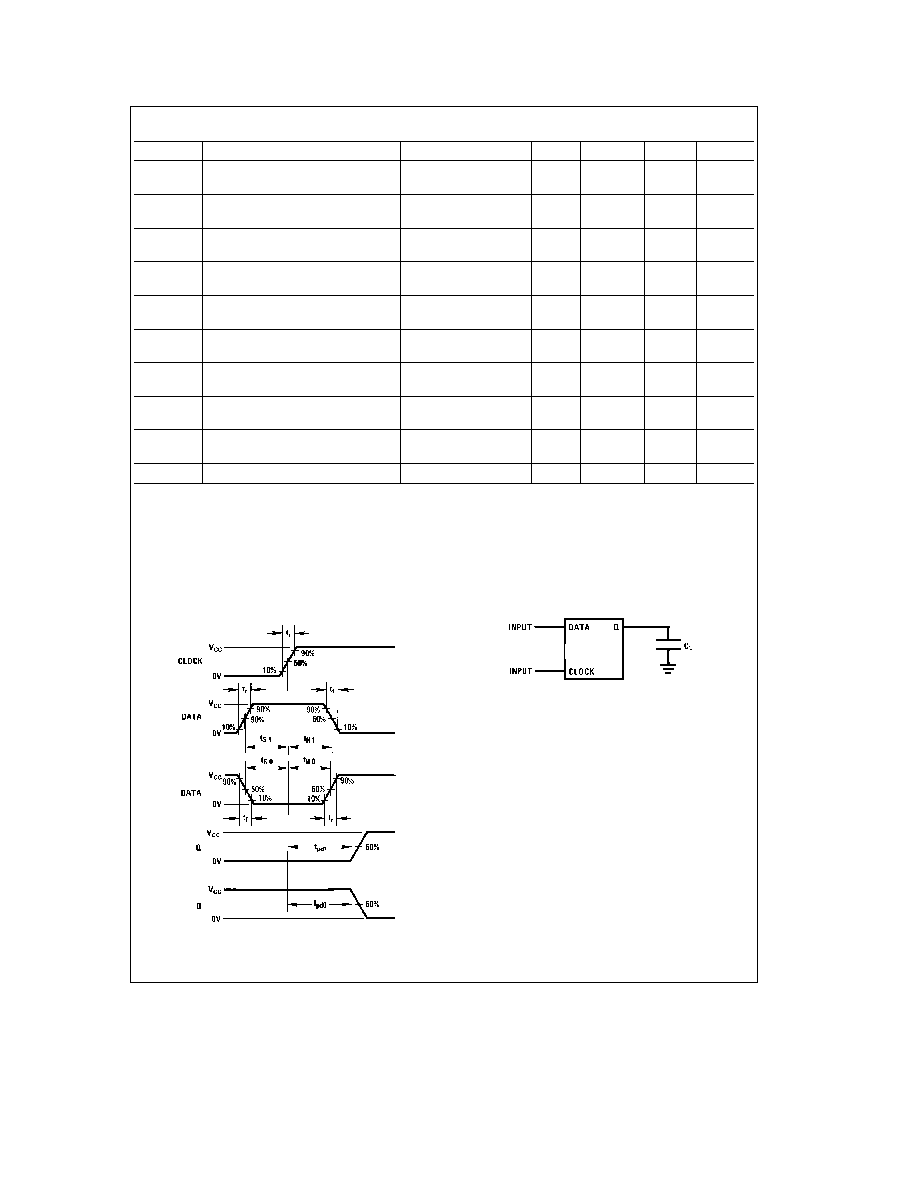
Switching Time Waveforms
CMOS to CMOS
TL F 5899 � 5
t
r
e
t
f
e
20 ns
AC Test Circuit
TL F 5899 � 6
3
MM54C174MM74C174
Hex
D
Flip-Flop
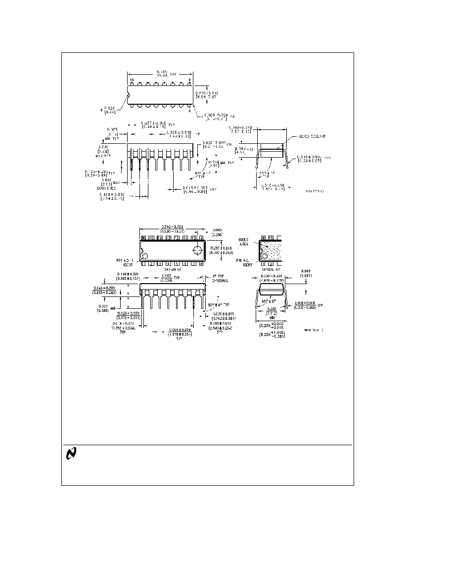
Physical Dimensions
inches (millimeters)
Ceramic Dual-In-Line Package (J)
Order Number MM54C174J or MM74C174J
NS Package Number J16A
Molded Dual-In-Line Package (N)
Order Number MM54C174N or MM74C174N
NS Package Number N16E
LIFE SUPPORT POLICY
NATIONAL'S PRODUCTS ARE NOT AUTHORIZED FOR USE AS CRITICAL COMPONENTS IN LIFE SUPPORT
DEVICES OR SYSTEMS WITHOUT THE EXPRESS WRITTEN APPROVAL OF THE PRESIDENT OF NATIONAL
SEMICONDUCTOR CORPORATION As used herein
1 Life support devices or systems are devices or
2 A critical component is any component of a life
systems which (a) are intended for surgical implant
support device or system whose failure to perform can
into the body or (b) support or sustain life and whose
be reasonably expected to cause the failure of the life
failure to perform when properly used in accordance
support device or system or to affect its safety or
with instructions for use provided in the labeling can
effectiveness
be reasonably expected to result in a significant injury
to the user
National Semiconductor
National Semiconductor
National Semiconductor
National Semiconductor
Corporation
Europe
Hong Kong Ltd
Japan Ltd
1111 West Bardin Road
Fax (a49) 0-180-530 85 86
13th Floor Straight Block
Tel 81-043-299-2309
Arlington TX 76017
Email cnjwge tevm2 nsc com
Ocean Centre 5 Canton Rd
Fax 81-043-299-2408
Tel 1(800) 272-9959
Deutsch Tel (a49) 0-180-530 85 85
Tsimshatsui Kowloon
Fax 1(800) 737-7018
English
Tel (a49) 0-180-532 78 32
Hong Kong
Fran ais Tel (a49) 0-180-532 93 58
Tel (852) 2737-1600
Italiano
Tel (a49) 0-180-534 16 80
Fax (852) 2736-9960
National does not assume any responsibility for use of any circuitry described no circuit patent licenses are implied and National reserves the right at any time without notice to change said circuitry and specifications