
TL F 5891
MM54C150MM74C150
16-Line
to
1-Line
Multiplexer
MM72C19MM82C19
TRI-STATE
16-Line
to
1-Line
Multiplexer
February 1988
MM54C150 MM74C150 16-Line to 1-Line Multiplexer
MM72C19 MM82C19 TRI-STATE
16-Line to 1-Line
Multiplexer
General Description
The MM54C150 MM74C150 and MM72C19 MM82C19
multiplex 16 digital lines to 1 output A 4-bit address code
determines the particular 1-of-16 inputs which is routed to
the output The data is inverted from input to output
A strobe override places the output of MM54C150
MM74C150 in the logical ``1'' state and the output of
MM72C19 MM82C19 in the high-impedance state
All inputs are protected from damage due to static dis-
charge by diode clamps to V
CC
and GND
Features
Y
Wide supply voltage range
3 0V to 15V
Y
Guaranteed noise margin
1 0V
Y
High noise immunity
0 45 V
CC
(typ )
Y
TTL compatibility
Drive 1 TTL Load
Connection Diagram
Dual-In-Line Package
TL F 5891 Ł 1
Order Number MM54C150 MM74C150 MM72C19 or MM82C19
TRI-STATE
is a registered trademark of National Semiconductor Corporation
C1995 National Semiconductor Corporation
RRD-B30M105 Printed in U S A
Absolute Maximum Ratings
(Note 1)
If Military Aerospace specified devices are required
please contact the National Semiconductor Sales
Office Distributors for availability and specifications
Voltage at Any Pin
b
0 3V to V
CC
a
0 3V
Operating Temperature Range
MM54C150 MM72C19
b
55 C to
a
125 C
MM74C150 MM82C19
b
40 C to
a
85 C
Storage Temperature Range
b
65 C to
a
150 C
Power Dissipation
Dual-In-Line
700 mW
Small Outline
500 mW
Operating V
CC
Range
3 0V to 15V
V
CC
18V
Lead Temperature (soldering 10 seconds)
260 C
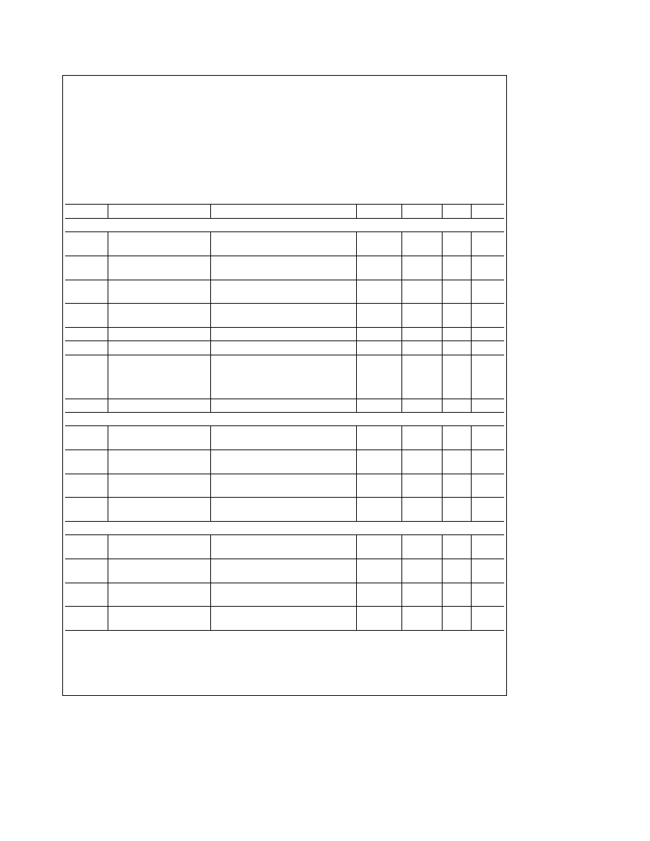
DC Electrical Characteristics
Min Max limits apply across temperature range unless otherwise noted
Symbol
Parameter
Conditions
Min
Typ
Max
Units
CMOS to CMOS
V
IN(1)
Logical ``1'' Input Voltage
V
CC
e
5 0V
3 5
V
V
CC
e
10V
8 0
V
V
IN(0)
Logical ``0'' Input Voltage
V
CC
e
5 0V
1 5
V
V
CC
e
10V
2 0
V
V
OUT(1)
Logical ``1'' Output Voltage
V
CC
e
5 0V I
O
e b
10 mA
4 5
V
V
CC
e
10V I
O
e b
10 mA
9 0
V
V
OUT(0)
Logical ``0'' Output Voltage
V
CC
e
5 0V I
O
e a
10 mA
0 5
V
V
CC
e
10V I
O
e a
10 mA
1 0
V
I
IN(1)
Logical ``1'' Input Current
V
CC
e
15V V
IN
e
15V
0 005
1 0
V
I
IN(0)
Logical ``0'' Input Current
V
CC
e
15V V
IN
e
0V
b
1 0
b
0 005
m
A
I
OZ
Output Current in High
Impedance State
MM72C19 MM82C19
V
CC
e
15V V
O
e
15V
0 005
1 0
m
A
V
CC
e
15V V
O
e
0V
b
1 0
b
0 005
m
A
I
CC
Supply Current
V
CC
e
15V
0 05
300
m
A
CMOS LPTTL Interface
V
IN(1)
Logical ``1'' Input Voltage
54C 72C V
CC
e
4 5V
V
CC
b
1 5
V
74C 82C V
CC
e
4 75V
V
CC
b
1 5
V
V
IN(0)
Logical ``0'' Input Voltage
54C 72C V
CC
e
4 5V
0 8
V
74C 82C V
CC
e
4 75V
0 8
V
V
OUT(1)
Logical ``1'' Output Voltage
54C 72C V
CC
e
4 5V I
O
e b
1 6 mA
2 4
V
74C 82C V
CC
e
4 75V I
O
e b
1 6 mA
2 4
V
V
OUT(0)
Logical ``0'' Output Voltage
54C 72C V
CC
e
4 5V I
O
e
1 6 mA
0 4
V
74C 82C V
CC
e
4 75V I
O
e
1 6 mA
0 4
V
Output Drive (Short Circuit Current)
I
SOURCE
Output Source Current
V
CC
e
5 0V V
OUT
e
0V T
A
e
25 C
b
4 35
b
8
mA
(P-Channel)
I
SOURCE
Output Source Current
V
CC
e
10V V
OUT
e
0V T
A
e
25 C
b
20
b
40
mA
(P-Channel)
I
SINK
Output Sink Current
V
CC
e
5 0V V
OUT
e
V
CC
T
A
e
25 C
4 35
8
mA
(N-Channel)
I
SINK
Output Sink Current
V
CC
e
10V V
OUT
e
V
CC
T
A
e
25 C
20
40
mA
(N-Channel)
Note 1
``Absolute Maximum Ratings'' are those values beyond which the safety of the device cannot be guaranteed Except for ``Operating Temperature Range''
they are not meant to imply that the devices should be operated at these limits The table of ``Electrical Characteristics'' provides conditions for actual device
operation
2
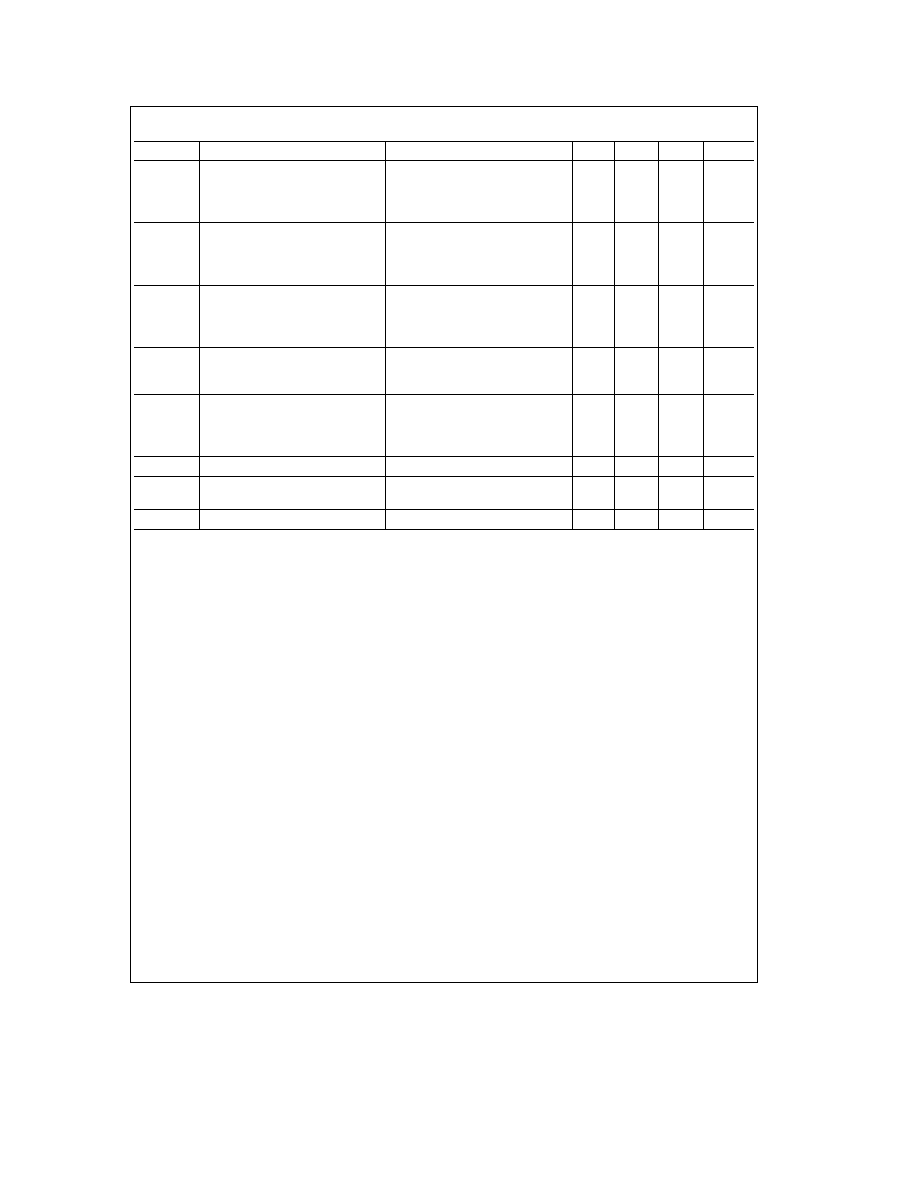
AC Electrical Characteristics
T
A
e
25 C C
L
e
50 pF unless otherwise noted
Symbol
Parameter
Conditions
Min
Typ
Max
Units
t
pd0
t
pd1
Propagation Delay Time to a
V
CC
e
5 0V
250
600
ns
Logical ``0'' or Logical ``1''
V
CC
e
10V
110
300
ns
from Data Inputs to Output
V
CC
e
5 0V C
L
e
150 pF
290
650
ns
V
CC
e
10V C
L
e
150 pF
120
330
ns
t
pd0
t
pd1
Propagation Delay Time to a
V
CC
e
5 0V
290
650
ns
Logical ``0'' or Logical ``1''
V
CC
e
10V
120
330
ns
from Data Select Inputs to
Output
t
pd0
t
pd1
Propagation Delay Time to a
V
CC
e
5 0V
120
300
ns
Logical ``0'' or Logical ``1''
V
CC
e
10V
55
150
ns
from Strobe to Output
MM54C150 MM74C150
t
1H
t
0H
Delay from Strobe to High
V
CC
e
5 0V R
L
e
10k C
L
e
5 pF
80
200
ns
Impedance State
V
CC
e
10V R
L
e
10k C
L
e
5 pF
60
150
ns
MM72C19 MM82C19
t
H1
t
H0
Delay from Strobe to Logical
V
CC
e
5 0V R
L
e
10k C
L
e
5 pF
80
250
ns
``1'' Level or to Logical ``0''
V
CC
e
10V R
L
e
10k C
L
e
5 pF
30
120
ns
Level (from High Impedance State)
MM72C19 MM82C19
C
IN
Input Capacitance
Any Input (Note 2)
5 0
pF
C
OUT
Output Capacitance
(Note 2)
11 0
pF
MM72C19 MM82C19
C
PD
Power Dissipation Capacitance
(Note 3)
100
pF
AC Parameters are guaranteed by DC correlated testing
Note 1
``Absolute Maximum Ratings'' are those values beyond which the safety of the device cannot be guaranteed Except for ``Operating Temperature Range''
they are not meant to imply that the devices should be operated at these limits The table of ``Electrical Characteristics'' provides conditions for actual device
operation
Note 2
Capacitance is guaranteed by periodic testing
Note 3
C
PD
determines the no load AC power consumption of any CMOS device For complete explanation see 54C 74C Family Characteristics application note
AN-90
3

Truth Table
MM54C150 MM74C150
Inputs
Output
D
C
B
A
STROBE
E0
E1
E2
E3
E4
E5
E6
E7
E8
E9
E10
E11
E12
E13
E14
E15
W
X
X
X
X
1
X
X
X
X
X
X
X
X
X
X
X
X
X
X
X
X
1
0
0
0
0
0
0
X
X
X
X
X
X
X
X
X
X
X
X
X
X
X
1
0
0
0
0
0
1
X
X
X
X
X
X
X
X
X
X
X
X
X
X
X
0
0
0
0
1
0
X
0
X
X
X
X
X
X
X
X
X
X
X
X
X
X
1
0
0
0
1
0
X
1
X
X
X
X
X
X
X
X
X
X
X
X
X
X
0
0
0
1
0
0
X
X
0
X
X
X
X
X
X
X
X
X
X
X
X
X
1
0
0
1
0
0
X
X
1
X
X
X
X
X
X
X
X
X
X
X
X
X
0
0
0
1
1
0
X
X
X
0
X
X
X
X
X
X
X
X
X
X
X
X
1
0
0
1
1
0
X
X
X
1
X
X
X
X
X
X
X
X
X
X
X
X
0
0
1
0
0
0
X
X
X
X
0
X
X
X
X
X
X
X
X
X
X
X
1
0
1
0
0
0
X
X
X
X
1
X
X
X
X
X
X
X
X
X
X
X
0
0
1
0
1
0
X
X
X
X
X
0
X
X
X
X
X
X
X
X
X
X
1
0
1
0
1
0
X
X
X
X
X
1
X
X
X
X
X
X
X
X
X
X
0
0
1
1
0
0
X
X
X
X
X
X
0
X
X
X
X
X
X
X
X
X
1
0
1
1
0
0
X
X
X
X
X
X
1
X
X
X
X
X
X
X
X
X
0
0
1
1
1
0
X
X
X
X
X
X
X
0
X
X
X
X
X
X
X
X
1
0
1
1
1
0
X
X
X
X
X
X
X
1
X
X
X
X
X
X
X
X
0
1
0
0
0
0
X
X
X
X
X
X
X
X
0
X
X
X
X
X
X
X
1
1
0
0
0
0
X
X
X
X
X
X
X
X
1
X
X
X
X
X
X
X
0
1
0
0
1
0
X
X
X
X
X
X
X
X
X
0
X
X
X
X
X
X
1
1
0
0
1
0
X
X
X
X
X
X
X
X
X
1
X
X
X
X
X
X
0
1
0
1
0
0
X
X
X
X
X
X
X
X
X
X
0
X
X
X
X
X
1
1
0
1
0
0
X
X
X
X
X
X
X
X
X
X
1
X
X
X
X
X
0
1
0
1
1
0
X
X
X
X
X
X
X
X
X
X
X
0
X
X
X
X
1
1
0
1
1
0
X
X
X
X
X
X
X
X
X
X
X
1
X
X
X
X
0
1
1
0
0
0
X
X
X
X
X
X
X
X
X
X
X
X
0
X
X
X
1
1
1
0
0
0
X
X
X
X
X
X
X
X
X
X
X
X
1
X
X
X
0
1
1
0
1
0
X
X
X
X
X
X
X
X
X
X
X
X
X
0
X
X
1
1
1
0
1
0
X
X
X
X
X
X
X
X
X
X
X
X
X
1
X
X
0
1
1
1
0
0
X
X
X
X
X
X
X
X
X
X
X
X
X
X
0
X
1
1
1
1
0
0
X
X
X
X
X
X
X
X
X
X
X
X
X
X
1
X
0
1
1
1
1
0
X
X
X
X
X
X
X
X
X
X
X
X
X
X
X
0
1
1
1
1
1
0
X
X
X
X
X
X
X
X
X
X
X
X
X
X
X
1
0
For MM72C19 MM82C19 this would be Hi-Z everything else is the same
Switching Time Waveforms
CMOS to CMOS
TL F 5891 Ł 2
4

Switching Time Waveforms
(Continued)
t
1H
and t
H1
TL F 5891 Ł 3
t
1H
TL F 5891 Ł 4
t
H1
TL F 5891 Ł 5
t
0H
and t
H0
TL F 5891 Ł 6
t
0H
TL F 5891 Ł 7
t
H0
Note
Delays measured with input t
r
t
f
s
20 ns
TL F 5891 Ł 8
5