TL F 11070
MM58167B
Microprocessor
Real
Time
Clock
October 1990
MM58167B
Microprocessor Real Time Clock
General Description
The MM58167B is a low threshold metal gate CMOS circuit
that functions as a real time clock in bus oriented microproc-
essor systems The device includes an addressable real
time counter 56 bits of RAM and two interrupt outputs A
POWER DOWN input allows the chip to be disabled from
the rest of the system for standby low power operation The
time base is a 32 768 kHz crystal oscillator
Features
Y
Microprocessor compatible (8-bit data bus)
Y
Milliseconds through month counters
Y
56 bits of RAM with comparator to compare the real
time counter to the RAM data
Y
2 INTERRUPT OUTPUTS with 8 possible interrupt
signals
Y
POWER DOWN input that disables all inputs and out-
puts except for one of the interrupts
Y
Status bit to indicate rollover during a read
Y
32 768 kHz crystal oscillator
Y
Four-year calendar (no leap year)
Y
24-hour clock
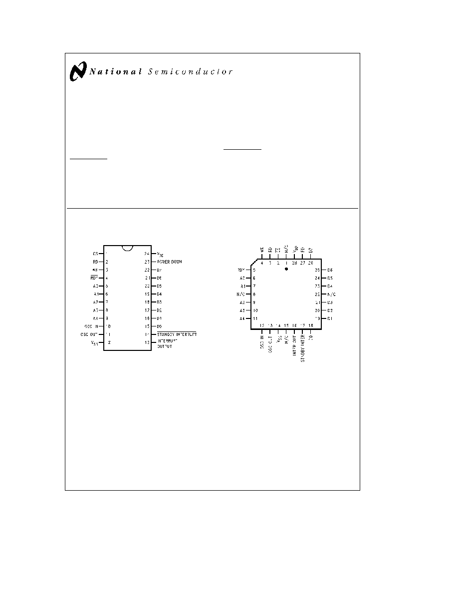
Connection Diagrams
Dual-In-Line Package
TL F 11070 Ł 1
Top View
Order Number MM58167BN
See NS Package Number N24A
PCC Package
TL F 11070 Ł 2
Top View
Order Number MM58167BV
See NS Package Number V28A
TRI-STATE
is a registered trademark of National Semiconductor Corporation
C1995 National Semiconductor Corporation
RRD-B30M105 Printed in U S A
Absolute Maximum Ratings
If Military Aerospace specified devices are required
please contact the National Semiconductor Sales
Office Distributors for availability and specifications
Voltage at All Pins
V
SS
b
0 3V to V
DD
a
0 3V
Operating Temperature
0 C to 70 C
Storage Temperature
b
65 C to
a
150 C
V
DD
b
V
SS
6 0V
Lead Temperature (Soldering 10 sec )
300 C
Electrical Characteristics
V
SS
e
0V 0 C
s
T
A
s
70 C
Parameter
Conditions
Min
Max
Units
Supply Voltage
V
DD
Outputs Enabled
4 5
5 5
V
V
DD
POWER DOWN Mode
2 2
5 5
V
Supply Current
I
DD
Dynamic
Outputs TRI-STATE
f
IN
e
32 768 kHz V
DD
e
5 5V
20
m
A
V
IH
t
V
DD
b
0 3V
V
IL
s
V
SS
a
0 3V
I
DD
Dynamic
Outputs TRI-STATE
f
IN
e
32 768 kHz V
DD
e
5 5V
5
mA
V
IH
e
2 0V V
IL
e
0 8V
Input Voltage
Logical Low
0 0
0 8
V
Logical high
2 0
V
DD
V
Input Leakage Current
V
SS
s
V
IN
s
V
DD
b
1
1
m
A
Output Impedance
I O and INTERRUPT OUT
Logical Low
V
DD
e
4 5V I
OL
e
1 6 mA
0 4
V
Logical High
V
DD
e
4 5V I
OH
e b
400 mA
2 4
V
I
OH
e b
10 mA
0 8 V
DD
V
TRI-STATE
V
SS
s
V
OUT
s
V
DD
b
1
1
m
A
Output Impedance
RDY and STANDBY INTERRUPT
(Open Drain Devices)
Logical Low Sink
V
DD
e
4 5V I
OL
e
1 6 mA
0 4
V
Logical High Leakage
V
OUT
s
V
DD
10
m
A
2
Functional Description
Real Time Counter
The real time counter is divided into 4-bit digits with 2 digits
being accessed during any read or write cycle Each digit
represents a BCD number and is defined in Table I Any
unused bits are held at a logical zero during a read and
ignored during a write An unused bit is any bit not neces-
sary to provide a full BCD number For example tens of
hours cannot legally exceed the number 2 thus only 2 bits
are necessary to define the tens of hours The other 2 bits in
the tens of hours digit are unused The unused bits are des-
ignated in Table I as dashes
The addressable portion of the counter is from milliseconds
to months The counter itself is a ripple counter The ripple
delay is less than 60 ms above 4 5V and 300 ms at 2 2V
RAM
56 bits of RAM are contained on-chip These can be used
for any necessary power down storage or as an alarm latch
for comparison to the real time counter The data in the
RAM can be compared to the real time counter on a digit
basis The only digits that are not compared are the unit ten
thousandths of seconds and tens of days of the week
(these are unused in the real time counter) If the two most
significant bits of any RAM digit are ones then this RAM
location will always compare The rule of thumb for an
``alarm'' interrupt is All nibbles of higher order than speci-
fied are set to C hex (always compare) All nibbles lower
than specified are set to ``zero'' As an example if an alarm
is to occur everyday at 10 15 a m configure the bits in RAM
as shown in Table II
The RAM is formatted the same as the real time counter 4
bits per digit 14 digits however there are no unused bits
The unused bits in the real time counter will compare only to
zeros in the RAM
An address map is shown in Table III
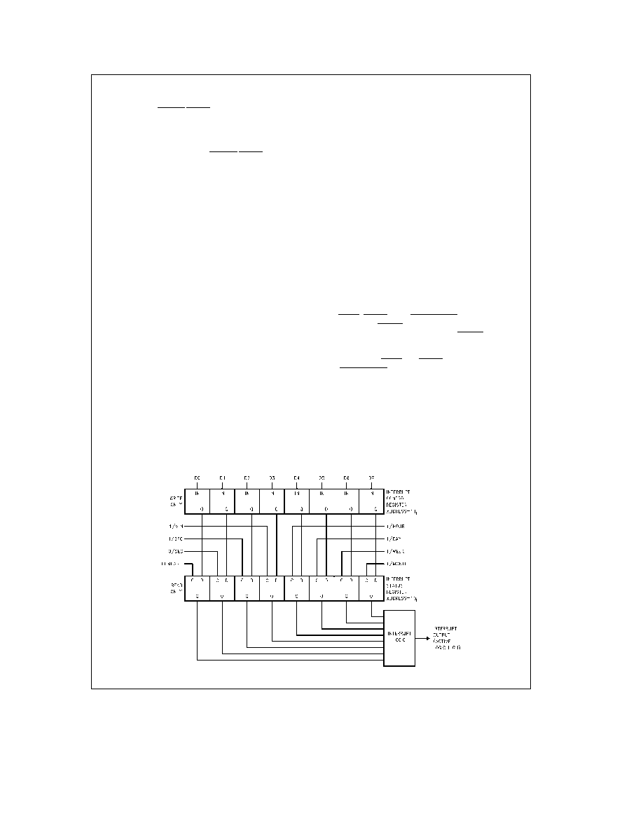
Interrupts and Comparator
There are two interrupt outputs The first is the INTERRUPT
OUTPUT (a true high signal) This output can be pro-
grammed to provide 8 different output signals They are
10 Hz once per second once per minute once per hour
once a day once a week once a month and when a RAM
real time counter comparison occurs To enable the output
a one is written into the interrupt control register at the bit
location corresponding to the desired output frequency (
Fig-
ure 1 ) Once one or more bits have been set in the interrupt
control register the corresponding counter's rollover to its
reset state will clock the interrupt status register and cause
the interrupt output to go high To reset the interrupt and to
identify which frequency caused the interrupt the interrupt
status register is read Reading this register places the con-
tents of the status register on the data bus The interrupting
frequency will be identified by a one in the respective bit
position Removing the read will reset the interrupt
The second interrupt is the STANDBY INTERRUPT (open
drain output active low) This interrupt occurs when enabled
and when a RAM real time counter comparison occurs The
STANDBY INTERRUPT is enabled by writing a one on the
D0 line at address 16
H
or disabled by writing a zero on the
D0 line This interrupt is not triggered by the edge of the
compare signal but rather by the level Thus if the compare
is enabled when the STANDBY INTERRUPT is enabled the
interrupt will turn on immediately
TABLE I Real Time Counter Format
Units
Max
Tens
Max
Counter Addressed
D0
D1
D2
D3
BCD
D4
D5
D6
D7
BCD
Code
Code
Milliseconds
(00
H
)
0
D4
D5
D6
D7
9
Hundredths and Tenths Sec
(01
H
)
D0
D1
D2
D3
9
D4
D5
D6
D7
9
Seconds
(02
H
)
D0
D1
D2
D3
9
D4
D5
D6
5
Minutes
(03
H
)
D0
D1
D2
D3
9
D4
D5
D6
5
Hours
(04
H
)
D0
D1
D2
D3
9
D4
D5
2
Day of the Week
(05
H
)
D0
D1
D2
7
0
Day of the Month
(06
H
)
D0
D1
D2
D3
9
D4
D5
3
Month
(07
H
)
D0
D1
D2
D3
9
D4
1
(
) indicates unused bits
3
Functional Description
(Continued)
TABLE II Clock RAM Bit Map for Alarm Interrupt Everyday at 10 15 a m
Address
Data
Function
Hi Nibble
Lo Nibble
4
3
2
1
0
7
6
5
4
3
2
1
0
Milliseconds
0
1
0
0
0
0
0
0
0
No RAM Exists
Hundredths and
0
1
0
0
1
0
0
0
0
0
0
0
0
Tenths of Seconds
Seconds
0
1
0
1
0
0
0
0
0
0
0
0
0
Minutes
0
1
0
1
1
0
0
0
1
0
1
0
1
Hours
0
1
1
0
0
0
0
0
1
0
0
0
0
Day of Week
0
1
1
0
1
No RAM Exists
1
1
X
X
Day of Month
0
1
1
1
0
1
1
X
X
1
1
X
X
Months
0
1
1
1
1
1
1
X
X
1
1
X
X
TABLE III Address Codes and Function
A4
A3
A2
A1
A0
Function
0
0
0
0
0
Counter
Milliseconds
0
0
0
0
1
Counter
Hundredths and Tenths of Seconds
0
0
0
1
0
Counter
Seconds
0
0
0
1
1
Counter
Minutes
0
0
1
0
0
Counter
Hours
0
0
1
0
1
Counter
Day of Week
0
0
1
1
0
Counter
Day of Month
0
0
1
1
1
Counter
Month
0
1
0
0
0
RAM
Milliseconds
0
1
0
0
1
RAM
Hundredths and Tenths of Seconds
0
1
0
1
0
RAM
Seconds
0
1
0
1
1
RAM
Minutes
0
1
1
0
0
RAM
Hours
0
1
1
0
1
RAM
Day of Week
0
1
1
1
0
RAM
Day of Month
0
1
1
1
1
RAM
Months
1
0
0
0
0
Interrupt Status Register
1
0
0
0
1
Interrupt Control Register
1
0
0
1
0
Counters Reset
1
0
0
1
1
RAM Reset
1
0
1
0
0
Status Bit
1
0
1
0
1
GO Comand
1
0
1
1
0
STANDBY INTERRUPT
1
1
1
1
1
Test Mode
All others unused
The comparator is a cascaded exclusive NOR Its output is
latched 61 ms after the rising edge of the 1 kHz clock signal
(input to the milliseconds counter) This allows the counter
to ripple through before looking at the comparator For oper-
ation at less than 4 5V the thousandths of seconds counter
should not be included in a compare because of the possi-
bility of having a ripple delay greater than 61 ms (For output
timing see Interrupt Timing )
Power Down Mode
The POWER DOWN input is essentially a second chip se-
lect
It disables all inputs and outputs except for the
STANDBY INTERRUPT When this input is at a logical zero
the device will not respond to any external signals It will
however maintain timekeeping and turn on the STANDBY
INTERRUPT if programmed to do so (The programming
must be done before the POWER DOWN input goes to a
4
Functional Description
(Continued)
logical zero ) When switching V
DD
to the standby or power
down mode the POWER DOWN input should go to a logical
zero at least 1 ms before V
DD
is switched When switching
V
DD
all other inputs must remain between V
SS
b
0 3V and
V
DD
a
0 3V When restoring V
DD
to the normal operating
mode it is necessary to insure that all other inputs are at
valid levels before switching the POWER DOWN input back
to a logical one These precautions are necessary to insure
that no data is lost or altered when changing to or from the
power down mode
Counter and RAM Resets GO Command
The counters and RAM can be reset by writing all 1's (FF) at
address 12
H
or 13
H
respectively
A write pulse at address 15
H
will reset the thousandths
hundredths tenths units and tens of seconds counters
This GO command is used for precise starting of the clock
The data on the data bus is ignored during the write If the
seconds counter is at a value greater than 39 when the GO
is issued the minute counter will increment otherwise the
minute counter is unaffected This command is not neces-
sary to start the clock but merely a convenient way to start
precisely at a given minute
Status Bit
The status bit is provided to inform the user that the clock is
in the process of rolling over when a counter is read The
status bit is set if this 1 kHz clock occurs during or after any
counter read This tells the user that the clock is rippling
through the real time counter Because the clock is rippling
invalid data may be read from the counter If the status bit is
set following a counter read the counter should be reread
The status bit appears on D0 when address 14
H
is read All
the other data lines will zero The bit is set when a logical
one appears This bit should be read every time a counter
read or after a series of counter reads are done The trailing
edge of the read at address 14
H
will reset the status bit
Using the Rollover Status Bit
If a single read of any clock counter is made it should be
followed by reading the rollover status bit
Example Read months then read rollover status
If a sequential read of the clock counters is made then the
rollover status bit should be read after the last counter is
read
Example Read hours minutes seconds then read the roll-
over status
Oscillator
The oscillator used is the standard Pierce parallel resonant
oscillator Externally 2 capacitors a 20 MX resistor and the
crystal are required The 20 MX resistor is connected be-
tween OSC IN and OSC OUT to bias the internal inverter in
the linear region For micropower crystals a resistor in series
with the oscillator output may be necessary to insure the
crystal is not overdriven This resistor should be approxi-
mately 200 kX The capacitor values should be typically
20 pF Ł 25 pF The crystal frequency is 32 768 Hz
The oscillator input can be externally driven if desired In
this case the oscillator output should be left floating and the
oscillator input levels should be within 0 3V of the supplies
A ground line or ground plane between pins 9 and 10 may
be necessary to reduce interference of the oscillator by the
A4 address
Control Lines
The READ WRITE AND CHIP SELECT signals are active
low inputs The READY signal is an open drain output At
the start of each read or write cycle the READY line (open
drain) will pull low and will remain low until valid data from a
chip read appears on the bus or data on the bus is latched
in during a write READ and WRITE must be accompanied
by a CHIP SELECT (see
Figures 3 and 4 for read and write
cycle timing)
During a read or write address bits must not change while
chip select and control strobes are low
Test Mode
The test mode is for production testing It allows the coun-
ters to count at a higher than normal rate In this mode the
32 768 kHz oscillator input is connected directly to the ten
thousandths of seconds counter The chip select and write
lines must be low and the address must be held at 1F
H
TL F 11070 Ł 3
FIGURE 1 Interrupt Register Format
5