
TL F 10821
MM5034MM5035
Octal
80-Bit
Static
Shift
Register
April 1990
MM5034 MM5035
Octal 80-Bit Static Shift Register
General Description
The MM5034 octal 80-bit shift register is a monolithic MOS
integrated circuit utilizing N-channel low threshold enhance-
ment mode and ion-implanted depletion mode devices
The MM5034 is designed for use in computer display pe-
ripherals All inputs and outputs are TTL compatible The
clocks and recirculate logic are internal to reduce system
component count and TRI-STATE
output buffers provide
bus interface Because of its N-channel characteristics sin-
gle 5V power supply operation is required
Simple interface to the NSC CRT DP8350 controller and
character generator to incorporate an entire CRT terminal is
feasible with the MM5034
The MM5034 is available in a 22-lead dual-in-line package
The MM5035 is a 20-pin version of the MM5034 with the
TRI-STATE output select feature omitted for a simple data
in data out operation
Features
Y
Single 5V power supply
Y
Internal clocks
Y
High speed and static operation
Y
TRI-STATE output buffer
Y
Recirculate and outut select independent
Y
TTL compatible
Applications
Y
CRT displays
Y
Computer peripherals
Connection Diagrams
Dual-In-Line Package
TL F 10821 � 1
Top View
Order Number MM5034N
See NS Package Number N22A
Dual-In-Line Package
TL F 10821 � 2
Top View
Order Number MM5035N
See NS Package Number N20A
TRI-STATE
is a registered trademark of National Semiconductor Corporation
C1995 National Semiconductor Corporation
RRD-B30M105 Printed in U S A
Absolute Maximum Ratings
If Military Aerospace specified devices are required
please contact the National Semiconductor Sales
Office Distributors for availability and specifications
Supply Voltage
7 V
DC
Input Voltage
7 V
DC
Power Dissipation
750 mW
Storage Temperature Range
b
65 C to
a
150 C
Lead Temperature (Soldering 10 sec )
300 C
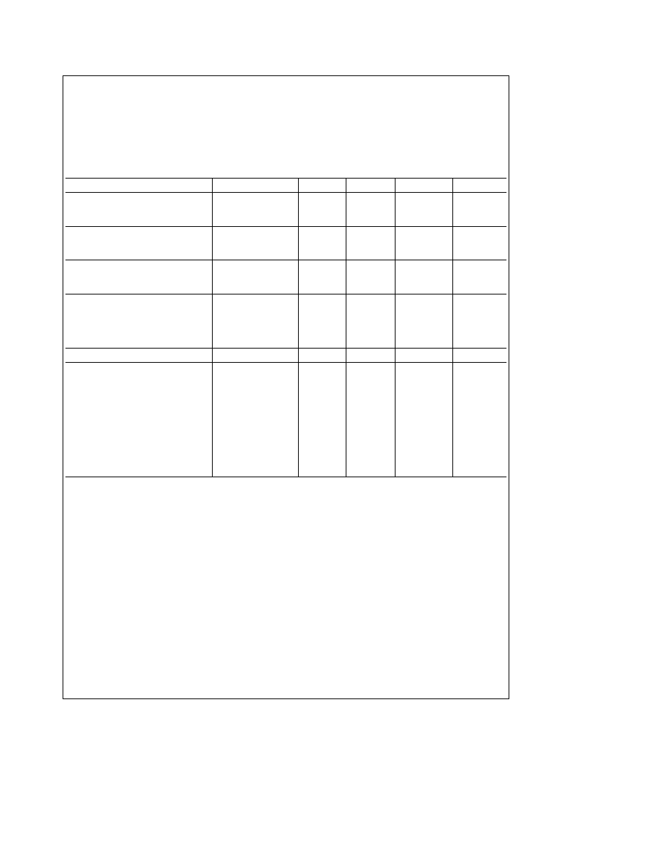
Electrical Characteristics
V
DD
e
5V
g
5% T
A
e
0 C to
a
70 C
Parameter
Conditions
Min
Typ
Max
Units
Clock Input
Logical ``1'' Input Voltage
2 2
V
Logical ``0'' Input Voltage
0 8
V
Data and Control Inputs
Logical ``1'' Input Voltage
2 2
V
Logical ``0'' Input Voltage
0 8
V
Data Clock and Control Inputs
Logical ``1'' Input Current
V
IN
e
5V
5 0
m
A
Input Capacitance
V
IN
e
2 5V
5 0
8 0
pF
Outputs
Logical ``1'' Output Voltage
I
OUT
e
100 mA
2 4
2 8
V
Logical ``0'' Output Voltage
I
OUT
e
1 6 mA
0 25
0 4
V
TRI-STATE Output Current
V
OUT
e
5V
b
5 0
m
A
V
OUT
e
0V
5 0
m
A
Supply Current
60
90
mA
Timing
Clock Frequency
0
3 0
MHz
Clock Pulse Width High
(Figure 1)
125
10 000
ns
Clock Pulse Width Low
(Note 1)
125
%
ns
Output Rise and Fall Time (t
r
t
f
)
(Figure 1)
40
50
ns
Set-Up Time
(Figure 1)
100
ns
Hold Time
(Figure 1)
0
ns
Output Enable Time
(Figure 1)
185
ns
Output Disable Time
(Figure 1)
185
ns
Clock Rise and Fall Time
(Figure 1)
5 0
m
s
Output Delay (t
PD
)
80
185
ns
Note 1
The clock input must be a low level for DC storage Minimum width assumes 10 ns t
r
and t
f
Recirculate and TRI-STATE Operation
Recirculate is used to maintain data in the shift register after
it has been loaded While the shift register is being loaded
Recirculate must be at a logical ``0'' When the loading is
completed Recirculate should be brought to a logical ``1''
This disables the data input and feeds the output of the last
shift cell back to the input of the first shift cell for each of the
8 registers
For the output to be in the TRI-STATE mode output-select
should be at the logical ``1'' level
2

AC Test Circuits and Switching Time Waveforms
t
PD1
TL F 10821 � 3
t
PD0
TL F 10821 � 4
TL F 10821 � 5
FIGURE 1
Typical Application
TL F 10821 � 6
FIGURE 2 CRT System Diagram Using the MM5034 MM5035 as a Line Buffer with DMA
3
MM5034MM5035
Octal
80-Bit
Static
Shift
Register
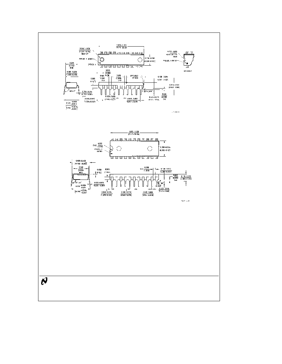
Physical Dimensions
inches (millimeters)
20-Lead Molded Dual-In-Line Package (N)
Order Number MM5035N
NS Package Number N20A
22-Lead Molded Dual-In-Line Package (N)
Order Number MM5034N
NS Package Number N22A
LIFE SUPPORT POLICY
NATIONAL'S PRODUCTS ARE NOT AUTHORIZED FOR USE AS CRITICAL COMPONENTS IN LIFE SUPPORT
DEVICES OR SYSTEMS WITHOUT THE EXPRESS WRITTEN APPROVAL OF THE PRESIDENT OF NATIONAL
SEMICONDUCTOR CORPORATION As used herein
1 Life support devices or systems are devices or
2 A critical component is any component of a life
systems which (a) are intended for surgical implant
support device or system whose failure to perform can
into the body or (b) support or sustain life and whose
be reasonably expected to cause the failure of the life
failure to perform when properly used in accordance
support device or system or to affect its safety or
with instructions for use provided in the labeling can
effectiveness
be reasonably expected to result in a significant injury
to the user
National Semiconductor
National Semiconductor
National Semiconductor
National Semiconductor
Corporation
Europe
Hong Kong Ltd
Japan Ltd
1111 West Bardin Road
Fax (a49) 0-180-530 85 86
13th Floor Straight Block
Tel 81-043-299-2309
Arlington TX 76017
Email cnjwge tevm2 nsc com
Ocean Centre 5 Canton Rd
Fax 81-043-299-2408
Tel 1(800) 272-9959
Deutsch Tel (a49) 0-180-530 85 85
Tsimshatsui Kowloon
Fax 1(800) 737-7018
English
Tel (a49) 0-180-532 78 32
Hong Kong
Fran ais Tel (a49) 0-180-532 93 58
Tel (852) 2737-1600
Italiano
Tel (a49) 0-180-534 16 80
Fax (852) 2736-9960
National does not assume any responsibility for use of any circuitry described no circuit patent licenses are implied and National reserves the right at any time without notice to change said circuitry and specifications