
LPV511
880 nA, Rail-to-Rail Input and Output Operational
Amplifier
General Description
The LPV511 is a micropower operational amplifier that op-
erates from a voltage supply range as wide as 2.7V to 12V
with guaranteed specifications at 3V, 5V and 12V. The
LPV511 exhibits an excellent speed to power ratio, drawing
only 880 nA of supply current with a bandwidth of 27 kHz.
These specifications make the LPV511 an ideal choice for
battery powered systems that require long life through low
supply current, such as instrumentation, sensor conditioning
and battery current monitoring.
The LPV511 has an input range that includes both supply
rails for ground and high side battery sensing applications.
The LPV511 output swings within 100 mV of either rail to
maximize the signal's dynamic range in low supply applica-
tions. In addition, the output is capable of sourcing 650 µA of
current when powered by a 12V battery.
The LPV511 is available in the space saving SC70 package
which makes it ideal for portable electronics with area con-
strained PC boards.
Features
(Typical at 3V supply unless otherwise noted)
n
Supply voltage range
2.7V to 12V
n
Slew rate
7.7 V/ms
n
Supply current
880 nA
n
Output short circuit current
1.35 mA
n
Rail-to-rail input
n
Output voltage swing
100 mV from rails
n
Bandwidth (C
L
= 50 pF, R
L
= 1 M
)
27 kHz
Applications
n
Battery powered systems
n
Security systems
n
Micropower thermostats
n
Solar powered systems
n
Portable instrumentation
n
Micropower filter
n
Remote sensor amplifier
Typical Application
20117003
August 2005
LPV51
1
880
nA,
Rail-to-Rail
Input
and
Output
Operational
Amplifier
© 2005 National Semiconductor Corporation
DS201170
www.national.com
Absolute Maximum Ratings
(Note 1)
If Military/Aerospace specified devices are required,
please contact the National Semiconductor Sales Office/
Distributors for availability and specifications.
ESD Tolerance (Note 2)
Human Body
2 KV
Machine Model
200V
V
IN
Differential
2.1V
Supply Voltage (V
+
- V
-
)
13.2V
Voltage at Input/Output pins
V
+
+0.3V, V
-
-0.3V
Storage Temperature Range
-65°C to +150°C
Short Circuit Duration
(Note 4)
Junction Temperature (Note 3)
+150°C
Soldering Information
Infrared or Convection (20 sec)
235°C
Wave Soldering Lead Temp. (10
sec)
260°C
Operating Ratings
(Note 1)
Temperature Range (Note 3)
-40°C to +85°C
Supply Voltage (V
+
V
-
)
2.7V to 12V
Package Thermal Resistance (
JA
(Note 3))
5-Pin SC70
456°C/W
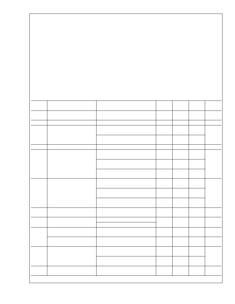
3V Electrical Characteristics
(Note 5)
Unless otherwise specified, all limits are guaranteed for T
J
= 25°C, V
+
= 3V, V
-
= 0V, V
CM
= V
O
= V
+
/2, and R
L
= 100 k
to
V
+
/2 . Boldface limits apply to the temperature range of -40°C to 85°C.
Symbol
Parameter
Conditions
Min
(Note 6)
Typ
(Note 7)
Max
(Note 6)
Units
V
OS
Input Offset Voltage
±
0.2
±
3
±
3.8
mV
TC V
OS
Input Offset Average Drift
(Note 8)
±
5
µV/C
I
B
Input Bias Current (Note 9)
V
CM
= 0.5V
-1000
1600
-320
pA
V
CM
= 2.5V
110
800
1900
I
OS
Input Offset Current
±
10
pA
CMRR
Common Mode Rejection Ratio
V
CM
Stepped from 0V to 1.5V
77
70
100
dB
V
CM
Stepped from 2.4V to 3V
75
68
115
V
CM
Stepped from 0.5V to 2.5V
60
56
80
PSRR
Power Supply Rejection Ratio
V
+
= 2.7V to 5V, V
CM
= 0.5V
72
68
114
dB
V
+
= 3V to 5V, V
CM
= 0.5V
76
72
115
V
+
= 5V to 12V, V
CM
= 0.5V
84
80
117
CMVR
Input Common-Mode Voltage
Range
CMRR
50 dB
-0.1
0
3.1
3.0
V
A
VOL
Large Signal Voltage Gain
Sinking, V
O
= 2.5V
75
70
105
dB
Sourcing, V
O
= 0.5V
V
O
Output Swing High
V
ID
= 100 mV
2.85
2.8
2.90
V
Output Swing Low
V
ID
= -100 mV
100
150
200
mV
I
SC
Output Short Circuit Current
(Note 10)
Sourcing
V
ID
= 100 mV
-500
-225
µA
Sinking
V
ID
= -100 mV
225
1350
I
S
Supply Current
0.88
1.2
1.5
µA
LPV51
1
www.national.com
2
3V Electrical Characteristics
(Note 5)
(Continued)
Unless otherwise specified, all limits are guaranteed for T
J
= 25°C, V
+
= 3V, V
-
= 0V, V
CM
= V
O
= V
+
/2, and R
L
= 100 k
to
V
+
/2 . Boldface limits apply to the temperature range of -40°C to 85°C.
Symbol
Parameter
Conditions
Min
(Note 6)
Typ
(Note 7)
Max
(Note 6)
Units
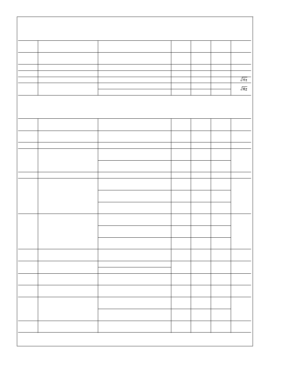
SR
Slew Rate (Note 11)
A
V
= +1, V
O
ramps from 0.5V to 2.5V
5.25
3.10
7.7
V/ms
GBW
Gain Bandwidth Product
R
L
= 1 M
, C
L
= 50 pF
27
kHz
Phase Margin
R
L
= 1 M
, C
L
= 50 pF
53
deg
e
n
Input-Referred Voltage Noise
f = 100 Hz
320
nV/
i
n
Input-Referred Current Noise
f = 10 Hz
.02
pA/
f = 1 kHz
.01
5V Electrical Characteristics
(Note 5)
Unless otherwise specified, all limits are guaranteed for T
J
= 25°C, V
+
= 5V, V
-
= 0V, V
CM
= V
O
= V
+
/2, and R
L
= 100 k
to
V
+
/2. Boldface limits apply to the temperature range of -40°C to 85°C.
Symbol
Parameter
Conditions
Min
(Note 6)
Typ
(Note 7)
Max
(Note 6)
Units
V
OS
Input Offset Voltage
±
0.2
±
3
±
3.8
mV
TC V
OS
Input Offset Average Drift
(Note 8)
±
5
µV/C
I
B
Input Bias Current (Note 9)
V
CM
= 0.5V
-1000
-1600
-320
pA
V
CM
= 4.5V
110
800
1900
I
OS
Input Offset Current
±
10
pA
CMRR
Common Mode Rejection Ratio
V
CM
Stepped from 0V to 2.5V
80
73
115
dB
V
CM
Stepped from 4.4 to 5V
75
68
107
V
CM
Stepped from 0.5 to 4.5V
65
62
87
PSRR
Power Supply Rejection Ratio
V
+
= 2.7V to 5V, V
CM
= 0.5V
72
68
114
dB
V
+
= 3V to 5V, V
CM
= 0.5V
76
72
115
V
+
= 5V to 12V, V
CM
= 0.5V
84
80
117
CMVR
Input Common-Mode Voltage
Range
CMRR
50 dB
-0.1
0
5.1
5
V
A
VOL
Large Signal Voltage Gain
Sinking, V
O
= 4.5V
78
73
110
dB
Sourcing, V
O
= 0.5V
V
O
Output Swing High
V
ID
= 100 mV
4.8
4.75
4.89
V
Output Swing Low
V
ID
= -100 mV
110
200
250
mV
I
SC
Output Short Circuit Current
(Note 10)
Sourcing to V
-
V
ID
= 100 mV
-550
-225
µA
Sinking to V
+
V
ID
= -100 mV
225
1350
I
S
Supply Current
0.97
1.2
1.5
µA
LPV51
1
www.national.com
3

5V Electrical Characteristics
(Note 5)
(Continued)
Unless otherwise specified, all limits are guaranteed for T
J
= 25°C, V
+
= 5V, V
-
= 0V, V
CM
= V
O
= V
+
/2, and R
L
= 100 k
to
V
+
/2. Boldface limits apply to the temperature range of -40°C to 85°C.
Symbol
Parameter
Conditions
Min
(Note 6)
Typ
(Note 7)
Max
(Note 6)
Units
SR
Slew Rate (Note 11)
A
V
= +1, V
O
ramps from 0.5V to 4.5V
5.25
3.10
7.5
V/ms
GBW
Gain Bandwidth Product
R
L
= 1 M
, C
L
= 50 pF
27
kHz
Phase Margin
R
L
= 1 M
, C
L
= 50 pF
53
deg
e
n
Input-Referred Voltage Noise
f = 100 Hz
320
nV/
i
n
Input-Referred Current Noise
f = 10 Hz
.02
pA/
f = 1 kHz
.01
12V Electrical Characteristics
(Note 5)
Unless otherwise specified, all limits are guaranteed for T
J
= 25°C, V
+
= 12V, V
-
= 0V, V
CM
= V
O
= V
+
/2, and R
L
= 100 k
to
V
+
/2. Boldface limits apply to the temperature range of -40°C to 85°C.
Symbol
Parameter
Conditions
Min
(Note 6)
Typ
(Note 7)
Max
(Note 6)
Units
V
OS
Input Offset Voltage
±
0.2
±
3
±
3.8
mV
TC V
OS
Input Offset Average Drift
(Note 8)
±
7
µV/C
I
B
Input Bias Current (Note 9)
V
CM
= 0.5V
-1000
-1600
-320
pA
V
CM
= 11.5V
110
800
1900
I
OS
Input Offset Current
±
10
pA
CMRR
Common Mode Rejection Ratio
V
CM
Stepped from 0V to +6V
75
70
115
dB
V
CM
Stepped from 11.4V to 12V
75
68
110
V
CM
Stepped from 0.5V to 11.5
70
65
97
PSRR
Power Supply Rejection Ratio
V
+
= 2.7V to 5V, V
CM
= 0.5V
72
68
114
dB
V
+
= 3V to 5V, V
CM
= 0.5V
76
72
115
V
+
= 5V to 12V, V
CM
= 0.5V
84
80
117
CMVR
Input Common-Mode Voltage
Range
CMRR
50 dB
-0.1
0
12.1
12
V
A
VOL
Large Signal Voltage Gain
Sinking, V
O
= 0.5V
89
84
110
dB
Sourcing, V
O
= 11.5V
V
O
Output Swing High
V
ID
= 100 mV
11.8
11.72
11.85
V
Output Swing Low
V
ID
= -100 mV
150
200
280
mV
I
SC
Output Short Circuit Current
(Note 10)
Sourcing
V
ID
= 100 mV
-650
-200
µA
Sinking
V
ID
= -100 mV
200
1300
I
S
Supply Current
1.2
1.75
2.5
µA
LPV51
1
www.national.com
4

12V Electrical Characteristics
(Note 5)
(Continued)
Unless otherwise specified, all limits are guaranteed for T
J
= 25°C, V
+
= 12V, V
-
= 0V, V
CM
= V
O
= V
+
/2, and R
L
= 100 k
to
V
+
/2. Boldface limits apply to the temperature range of -40°C to 85°C.
Symbol
Parameter
Conditions
Min
(Note 6)
Typ
(Note 7)
Max
(Note 6)
Units
SR
Slew Rate (Note 11)
A
V
= +1, V
O
ramped from 1V to 11V
5.25
3.10
7.0
V/ms
GBW
Gain Bandwidth Product
R
L
= 1 M
, C
L
= 50 pF
25
kHz
Phase Margin
R
L
= 1 M
, C
L
= 50 pF
52
deg
e
n
Input-Referred Voltage Noise
f = 100 Hz
320
nV/
i
n
Input-Referred Current Noise
f = 10 Hz
.02
pA/
f = 1 kHz
.01
Note 1: Absolute Maximum Ratings indicate limits beyond which damage to the device may occur. Operating Ratings indicate conditions for which the device is
intended to be functional, but specific performance is not guaranteed. For guaranteed specifications and the test conditions, see the Electrical Characteristics Tables.
Note 2: Human Body Model: 1.5 k
in series with 100 pF. Machine Model: 0 in series with 200 pF.
Note 3: The maximum power dissipation is a function of T
J(MAX)
,
JA
, and T
A
. The maximum allowable power dissipation at any ambient temperature is
P
D
= (T
J(MAX)
- T
A
)/
JA
. All numbers apply for packages soldered directly onto a PC board.
Note 4: Output short circuit duration is infinite for V
+
<
6V at room temperature and below. For V
+
>
6V, allowable short circuit duration is 1.5 ms.
Note 5: Electrical table values apply only for factory testing conditions at the temperature indicated. Factory testing conditions result in very limited self-heating of
the device.
Note 6: Limits are 100% production tested at 25°C. Limits over the operating temperature range are guaranteed through correlations using the Statistical Quality
Control (SQC) method.
Note 7: Typical values represent the most likely parametric norm at the time of characterization.
Note 8: Offset voltage average drift is determined by dividing the change in V
OS
at temperature extremes into the total temperature change.
Note 9: Positive current corresponds to current flowing into the device.
Note 10: The Short Circuit Test is a momentary test. See (Note 4).
Note 11: Slew rate is the average of the rising and falling slew rates.
LPV51
1
www.national.com
5