LMV761/LMV762
Low Voltage, Precision Comparator with Push-Pull
Output
General Description
The LMV761/762 are precision comparators intended for
applications requiring low noise and low input offset voltage.
The LV761 single has a shutdown pin that can be used to
disable the device and reduce the supply current. The
LMV761 is available in a space saving SOT23-6 or SOIC-8
package. The LMV762 dual is available in SOIC-8 or
MSOP-8 package.
They feature a CMOS input and Push-Pull output stage. The
Push-Pull output stage eliminates the need for an external
pull-up resistor.
The LMV761/762 are designed to meet the demands of
small size, low power and high performance required by
portable and battery operated electronics.
The input offset voltage has a typical value of 200µV at room
temp and a 1mV limit over temp.
Features
(V
S
= 5V, T
A
= 25°C, Typical values unless specified)
n
Input offset voltage
0.2mV
n
Input offset voltage (max over temp)
1mV
n
Input bias current
0.2pA
n
Propagation delay (OD = 50mV)
120 nsec
n
Low supply current
300µA
n
CMRR
100dB
n
PSRR
110dB
n
Extended Temperature Range
-40°C to 125°C
n
Push-pull output
n
Ideal for 2.7V and 5V single supply applications
n
Available in space-saving packages:
6-Pin SOT23 (single w/shutdown)
8-Pin SOIC (single w/shutdown)
8-Pin SOIC/MSOP (dual without shutdown)
Applications
n
Portable and battery-powered systems
n
Scanners
n
Set top boxes
n
High speed differential line receiver
n
Window comparators
n
Zero-crossing detectors
n
High speed sampling circuits
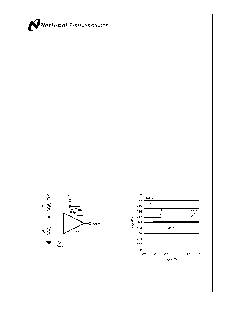
Typical Circuit
20037032
Threshold Detector
V
OS
vs. V
CC
20037010
July 2002
LMV761/LMV762
Low
V
oltage,
Precision
Comparator
with
Push-Pull
Output
© 2002 National Semiconductor Corporation
DS200370
www.national.com
Absolute Maximum Ratings
(Note 1)
If Military/Aerospace specified devices are required,
please contact the National Semiconductor Sales Office/
Distributors for availability and specifications.
ESD Tolerance (Note 2)
Human Body Model
2000V
Machine Model
200V
Supply Voltage (V
+
V
-
)
5.5V
Differential Input Voltage
Supply Voltage
Voltage between any two pins
Supply Voltage
Output Short Circuit to V
+
- V
-
Soldering Information
Infrared or Convection (20 sec.)
235°C
Wave Soldering (10 sec.)
260°C (Lead Temp)
Junction Temperature
150°C
Storage Temperature Range
-65°C to 150°C
Operating Ratings
Supply Voltage (V
+
V
-
)
2.7V to 5.0V
Temperature Range
-40°C to +125°C
Package Thermal Resistance (Note 4)
SOT23-6
265°C/W
SOIC-8
190°C/W
MSOP-8
235°C/W
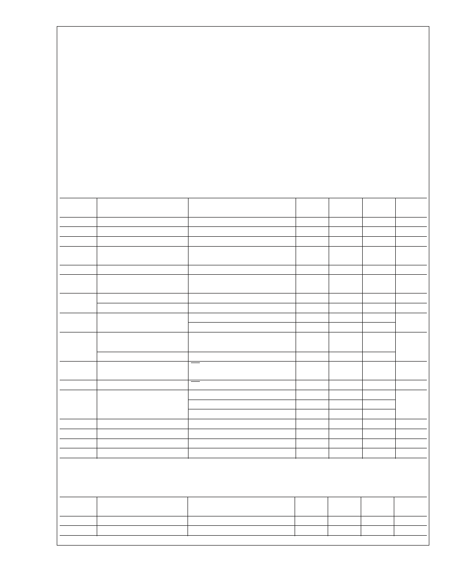
2.7V Electrical Characteristics
Unless otherwise specified, all limited guaranteed for T
J
= 25°C, V
CM
= V
+
/2, V
+
= 2.7V, V
-
= 0V
-
. Boldface limits apply at the
temperature extremes. (Note 5)
Symbol
Parameter
Condition
Min
(Note 7)
Typ
(Note 6)
Max
(Note 7)
Units
V
OS
Input Offset Voltage
0.2
1.0
mV
I
B
Input Bias Current (Note 8)
0.2
50
pA
I
OS
Input Offset Current (Note 8)
.001
5
pA
CMRR
Common Mode Rejection
Ratio
0V
<
V
CM
<
V
CC
- 1.3V
80
100
dB
PSRR
Power Supply Rejection Ratio
V
+
= 2.7V to 5V
80
110
dB
CMVR
Input Common Mode Voltage
Range
CMRR
>
50dB
-0.3
1.5
V
V
O
Output Swing High
I
L
= 2mA, V
ID
= 200mV
V
+
0.35
V
+
0.1
V
Output Swing Low
I
L
= -2mA, V
ID
= -200mV
90
250
mV
I
SC
Output Short Circuit Current
(Note 3)
Sourcing, V
O
= 1.35V, V
ID
= 200mV
6.0
20
mA
Sinking, V
O
= 1.35V, V
ID
= -200mV
6.0
15
I
S
Supply Current
µA
LMV761 (Single Comparator)
275
700
LMV762 (Both Comparators)
550
1400
I
OUT
LEAKAGE
Output Leakage I
@
Shutdown
SD = GND, V
O
= 2.7V
0.20
µA
I
S LEAKAGE
Supply Leakage I
@
Shutdown
SD = GND, V
CC
= 2.7V
0.20
2
µA
t
PD
Propagation Delay
R
L
= 5.1k
C
L
= 50pF
Overdrive = 5mV
270
ns
Overdrive = 10mV
205
Overdrive = 50mV
120
t
SKEW
Propagation Delay Skew
5
ns
t
r
Output Rise Time
10% to 90%
1.7
ns
t
f
Output Fall Time
90% to 10%
1.8
ns
t
on
Turn On Time From Shutdown
6
µs
5.0V Electrical Characteristics
Unless otherwise specified, all limited guaranteed for T
J
= 25°C, V
CM
= V
+
/2, V
+
= 5.0V, V
-
= 0V
-
. Boldface limits apply at the
temperature extremes.
Symbol
Parameter
Condition
Min
(Note 7)
Typ
(Note 6)
Max
(Note 7)
Units
V
OS
Input Offset Voltage
0.2
1.0
mV
I
B
Input Bias Current (Note 8)
0.2
50
pA
LMV761/LMV762
www.national.com
2

5.0V Electrical Characteristics
(Continued)
Unless otherwise specified, all limited guaranteed for T
J
= 25°C, V
CM
= V
+
/2, V
+
= 5.0V, V
-
= 0V
-
. Boldface limits apply at the
temperature extremes.
Symbol
Parameter
Condition
Min
(Note 7)
Typ
(Note 6)
Max
(Note 7)
Units
I
OS
Input Offset Current (Note 8)
0.01
5
pA
CMRR
Common Mode Rejection
Ratio
0V
<
V
CM
<
V
CC
- 1.3V
80
100
dB
PSRR
Power Supply Rejection Ratio
V
+
= 2.7V to 5V
80
110
dB
CMVR
Input Common Mode Voltage
Range
CMRR
>
50dB
-.3
3.8
V
V
O
Output Swing High
I
L
= 4mA, V
ID
= 200mV
V
+
0.35
V
+
0.1
V
Output Swing Low
I
L
= -4mA, V
ID
= -200mV
120
250
mV
I
SC
Output Short Circuit Current
(Note 3)
Sourcing, V
O
= 2.5V, V
ID
= 200mV
6.0
60
mA
Sinking, V
O
= 2.5V, V
ID
= -200mV
6.0
40
I
S
Supply Current
µA
LMV761 (Single Comparator)
225
700
LMV762 (Both Comparators)
450
1400
I
OUT
LEAKAGE
Output Leakage I
@
Shutdown
SD = GND, V
O
= 5.0V
0.20
µA
I
S LEAKAGE
Supply Leakage I
@
Shutdown
SD = GND, V
CC
= 5.0V
0.20
2
µA
t
PD
Propagation Delay
R
L
= 5.1k
C
L
= 50pF
Overdrive = 5mV
225
ns
Overdrive = 10mV
190
Overdrive = 50mV
120
t
SKEW
Propagation Delay Skew
5
ns
t
r
Output Rise Time
10% to 90%
1.7
ns
t
f
Output Fall Time
90% to 10%
1.5
ns
t
on
Turn On Time from Shutdown
4
µs
Note 1: Absolute Maximum Ratings indicate limits beyond which damage to the device may occur. Operating Ratings indicate conditions for which the device is
intended to be functional, but specific performance is not guaranteed. For guaranteed specifications and the test condition, see the Electrical Characteristics.
Note 2: Unless otherwise specified human body model is 1.5k
in series with 100pF. Machine model 200pF.
Note 3: Electrical Table values apply only for factory testing conditions at the temperature indicated. Factory testing conditions result in very limited self-heating of
the device such that T
J
= T
A
. No guarantee of parametric performance is indicated in the electrical tables under conditions of internal self-heating where T
J
>
T
A
.
See Application section for information on temperature de-rating of this device. Absolute Maximum Rating indicate junction temperature limits beyond which the
device may be permanently degraded, either mechanically or electrically.
Note 4: The maximum power dissipation is a function of T
J(MAX
),
JA
, and T
A
. The maximum allowable power dissipation at any ambient temperature is
P
D
= (T
J(MAX)
-T
A
)
JA
. All numbers apply for packages soldered directly into a PC board.
Note 5: Maximum temperature guarantee range is -40°C to 125°C.
Note 6: Typical values represent the most likely parametric norm.
Note 7: All limits are guaranteed by testing or statistical analysis.
Note 8: Guaranteed by design
LMV761/LMV762
www.national.com
3

Connection Diagrams
LMV761
Single 6-Pin SOT23
LMV761
Single 8-Pin SOIC
LMV762
Dual 8-Pin SOIC & MSOP
20037001
Top View
20037002
Top View
20037003
Top View
Ordering Information
Package
Part Number
Package Marking
Transport Media
NSC Drawing
6-Pin SOT23
LMV761MF
C22A
1k units Tape and Reel
MF06A
LMV761MFX
3k units Tape and Reel
8-Pin SOIC
LMV761MA
LMV761MA
Rail
M08A
LMV761MAX
2.5k Units Tape and Reel
8-Pin SOIC
LMV762MA
LMV762MA
Rail
M08A
LMV762MAX
2.5k Units Tape and Reel
8-Pin MSOP
LMV762MM
C23A
1k Units Tape and Reel
MUA08A
LMV762MMX
3.5k Units Tape and Reel
LMV761/LMV762
www.national.com
4
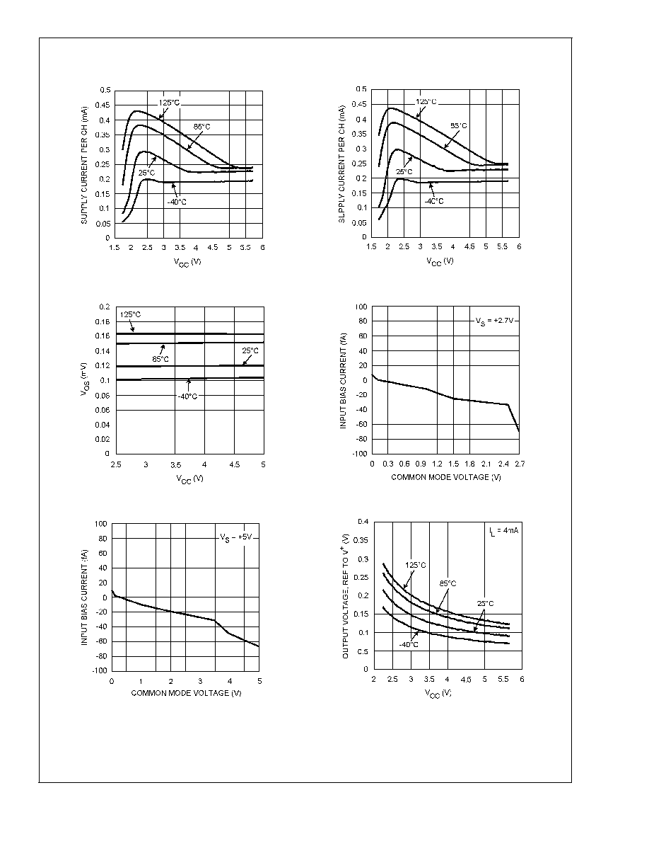
Typical Performance Characteristics
PSI vs. V
CC
(V
O
= High)
PSI vs. V
CC
(V
O
= Low)
20037004
20037005
V
OS
vs. V
CC
Input Bias vs. Common Mode
@
25°C
20037010
20037024
Input Bias vs. Common Mode
@
25°C
Output Voltage vs. Supply Voltage
20037025
20037011
LMV761/LMV762
www.national.com
5