
LMP7711/LMP7712
Single and Dual Precision, 17 MHz, Low Noise, CMOS
Input Amplifiers
General Description
The LMP7711/LMP7712 are single and dual low noise, low
offset, CMOS input, rail-to-rail output precision amplifiers
with a high gain bandwidth product and an enable pin. The
LMP7711/LMP7712 are part of the LMP
TM
precision amplifier
family and are ideal for a variety of instrumentation applica-
tions.
Utilizing a CMOS input stage, the LMP7711/LMP7712
achieve an input bias current of 100 fA, an input referred
voltage noise of 5.8 nV/
, and an input offset voltage of
less than
±
150 µV. These features make the LMP7711/
LMP7712 superior choices for precision applications.
Consuming only 1.15 mA of supply current, the LMP7711
offers a high gain bandwidth product of 17 MHz, enabling
accurate amplification at high closed loop gains.
The LMP7711/LMP7712 have a supply voltage range of
1.8V to 5.5V, which makes these ideal choices for portable
low power applications with low supply voltage require-
ments. In order to reduce the already low power consump-
tion the LMP7711/LMP7712 have an enable function. Once
in shutdown, the LMP7711/LMP7712 draw only 140 nA of
supply current.
The LMP7711/LMP7712 are built with National's advanced
VIP50 process technology. The LMP7711 is offered in a
6-pin TSOT23 package and the LMP7712 is offered in a
10-pin MSOP.
Features
Unless otherwise noted, typical values at V
S
= 5V.
n
Input offset voltage
±
150 µV (max)
n
Input bias current
100 fA
n
Input voltage noise
5.8 nV/
n
Gain bandwidth product
17 MHz
n
Supply current (LMP7711)
1.15 mA
n
Supply current (LMP7712)
1.30 mA
n
Supply voltage range
1.8V to 5.5V
n
THD+N
@
f = 1 kHz
0.001%
n
Operating temperature range
-40
o
C to 125°C
n
Rail-to-rail output swing
n
Space saving TSOT23 package (LMP7711)
n
MSOP-10 package (LMP7712)
Applications
n
Active filters and buffers
n
Sensor interface applications
n
Transimpedance amplifiers
Typical Performance
Offset Voltage Distribution
Input Referred Voltage Noise
20150322
20150339
LMP
TM
is a trademark of National Semiconductor Corporation.
November 2005
LMP771
1/LMP7712
Precision,
17
MHz,
Low
Noise,
CMOS
Input
Amplifiers
© 2005 National Semiconductor Corporation
DS201503
www.national.com
Absolute Maximum Ratings
(Note 1)
If Military/Aerospace specified devices are required,
please contact the National Semiconductor Sales Office/
Distributors for availability and specifications.
ESD Tolerance (Note 2)
Human Body Model
2000V
Machine Model
200V
V
IN
Differential
±
0.3V
Supply Voltage (V
S
= V
+
V
-
)
6.0V
Voltage on Input/Output Pins
V
+
+0.3V, V
-
-0.3V
Storage Temperature Range
-65°C to 150°C
Junction Temperature (Note 3)
+150°C
Soldering Information
Infrared or Convection (20 sec)
235°C
Wave Soldering Lead Temp. (10
sec)
260°C
Operating Ratings
(Note 1)
Temperature Range (Note 3)
-40°C to 125°C
Supply Voltage (V
S
= V
+
V
-
)
0°C
T
A
125°C
1.8V to 5.5V
-40°C
T
A
125°C
2.0V to 5.5V
Package Thermal Resistance (
JA
(Note 3))
6-Pin TSOT23
170°C/W
10-Pin MSOP
236°C/W
2.5V Electrical Characteristics
Unless otherwise specified, all limits are guaranteed for T
A
= 25°C, V
+
= 2.5V, V
-
= 0V ,V
O
= V
CM
= V
+
/2, V
EN
= V
+
. Boldface
limits apply at the temperature extremes.
Symbol
Parameter
Conditions
Min
(Note 5)
Typ
(Note 4)
Max
(Note 5)
Units
V
OS
Input Offset Voltage
±
20
±
180
±
480
µV
TC V
OS
Input Offset Voltage Drift
(Note 6)
LMP7711
1
±
4
µV/°C
LMP7712
1.75
I
B
Input Bias Current
V
CM
= 1V
(Notes 7, 8)
0.05
50
100
pA
I
OS
Input Offset Current
V
CM
= 1V
(Note 8)
0.006
25
50
pA
CMRR
Common Mode Rejection Ratio
0V
V
CM
1.4V
83
80
100
dB
PSRR
Power Supply Rejection Ratio
2.0V
V
+
5.5V
V
-
= 0V, V
CM
= 0
85
80
100
dB
1.8V
V
+
5.5V
V
-
= 0V, V
CM
= 0
85
98
CMVR
Input Common-Mode Voltage
Range
CMRR
80 dB
CMRR
78 dB
-0.3
0.3
1.5
1.5
V
A
VOL
Large Signal Voltage Gain
LMP7711, V
O
= 0.15 to 2.2V
R
L
= 2 k
to V
+
/2
88
82
98
dB
LMP7712, V
O
= 0.15 to 2.2V
R
L
= 2 k
to V
+
/2
84
80
92
LMP7711, V
O
= 0.15 to 2.2V
R
L
= 10 k
to V
+
/2
92
88
110
LMP7712, V
O
= 0.15 to 2.2V
R
L
= 10 k
to V
+
/2
90
86
95
V
O
Output Swing High
R
L
= 2 k
to V
+
/2
70
77
25
mV
from V
+
R
L
= 10 k
to V
+
/2
60
66
20
Output Swing Low
R
L
= 2 k
to V
+
/2
30
70
73
mV
R
L
= 10 k
to V
+
/2
15
60
62
LMP771
1/LMP7712
www.national.com
2
2.5V Electrical Characteristics
(Continued)
Unless otherwise specified, all limits are guaranteed for T
A
= 25°C, V
+
= 2.5V, V
-
= 0V ,V
O
= V
CM
= V
+
/2, V
EN
= V
+
. Boldface
limits apply at the temperature extremes.
Symbol
Parameter
Conditions
Min
(Note 5)
Typ
(Note 4)
Max
(Note 5)
Units
I
O
Output Short Circuit Current
Sourcing to V
-
V
IN
= 200 mV (Note 9)
36
30
52
mA
Sinking to V
+
V
IN
= -200 mV (Note 9)
7.5
5.0
15
I
S
Supply Current
LMP7711
Enable Mode V
EN
2.1
0.95
1.30
1.65
mA
LMP7712 (per channel)
Enable Mode V
EN
2.1
1.10
1.50
1.85
Shutdown Mode (per channel)
V
EN
0.4
0.03
1
4
µA
SR
Slew Rate
A
V
= +1, Rising (10% to 90%)
8.3
V/µs
A
V
= +1, Falling (90% to 10%)
10.3
GBW
Gain Bandwidth Product
14
MHz
e
n
Input-Referred Voltage Noise
f = 400 Hz
6.8
nV/
f = 1 kHz
5.8
i
n
Input-Referred Current Noise
f = 1 kHz
0.01
pA/
t
on
Turn-on Time
140
ns
t
off
Turn-off Time
1000
ns
V
EN
Enable Pin Voltage Range
Enable Mode
2.1
2 - 2.5
V
Shutdown Mode
0 - 0.5
0.4
I
EN
Enable Pin Input Current
V
EN
= 2.5V (Note 7)
1.5
3.0
µA
V
EN
= 0V (Note 7)
0.003
0.1
THD+N
Total Harmonic Distortion +
Noise
f = 1 kHz, A
V
= 1, R
L
= 100 k
V
O
= 0.9 V
PP
0.003
%
f = 1 kHz, A
V
= 1, R
L
= 600
V
O
= 0.9 V
PP
0.004
5V Electrical Characteristics
Unless otherwise specified, all limits are guaranteed for T
A
= 25°C, V
+
= 5V, V
-
= 0V, V
CM
= V
+
/2, V
EN
= V
+
. Boldface limits
apply at the temperature extremes.
Symbol
Parameter
Conditions
Min
(Note 5)
Typ
(Note 4)
Max
(Note 5)
Units
V
OS
Input Offset Voltage
±
10
±
150
±
450
µV
TC V
OS
Input Offset Average Drift
(Note 6)
LMP7711
1
±
4
µV/°C
LMP7712
1.75
I
B
Input Bias Current
(Notes 7, 8)
0.1
50
100
pA
I
OS
Input Offset Current
(Note 8)
0.01
25
50
pA
CMRR
Common Mode Rejection
Ratio
0V
V
CM
3.7V
85
82
100
dB
PSRR
Power Supply Rejection Ratio
2.0V
V
+
5.5V
V
-
= 0V, V
CM
= 0
85
80
100
dB
1.8V
V
+
5.5V
V
-
= 0V, V
CM
= 0
85
98
CMVR
Input Common-Mode Voltage
Range
CMRR
80 dB
CMRR
78 dB
-0.3
0.3
4
4
V
LMP771
1/LMP7712
www.national.com
3

5V Electrical Characteristics
(Continued)
A
VOL
Large Signal Voltage Gain
LMP7711, V
O
= 0.3 to 4.7V
R
L
= 2 k
to V
+
/2
88
82
107
dB
LMP7712, V
O
= 0.3 to 4.7V
R
L
= 2 k
to V
+
/2
84
80
90
LMP7711, V
O
= 0.3 to 4.7V
R
L
= 10 k
to V
+
/2
92
88
110
LMP7712, V
O
= 0.3 to 4.7V
R
L
= 10 k
to V
+
/2
90
86
95
V
O
Output Swing High
R
L
= 2 k
to V
+
/2
70
77
32
mV
from V
+
R
L
= 10 k
to V
+
/2
60
66
22
Output Swing Low
R
L
= 2 k
to V
+
/2
(LMP7711)
42
70
73
mV
R
L
= 2 k
to V
+
/2
(LMP7712)
50
75
78
R
L
= 10 k
to V
+
/2
20
60
62
I
O
Output Short Circuit Current
Sourcing to V
-
V
IN
= 200 mV (Note 9)
46
38
66
mA
Sinking to V
+
V
IN
= -200 mV (Note 9)
10.5
6.5
23
I
S
Supply Current
LMP7711
Enable Mode V
EN
4.6
1.15
1.40
1.75
mA
LMP7712 (per channel)
Enable Mode V
EN
4.6
1.30
1.70
2.05
Shutdown Mode V
EN
0.4
(per channel)
0.14
1
4
µA
SR
Slew Rate
A
V
= +1, Rising (10% to 90%)
6.0
9.5
V/µs
A
V
= +1, Falling (90% to 10%)
7.5
11.5
GBW
Gain Bandwidth Product
17
MHz
e
n
Input-Referred Voltage Noise
f = 400 Hz
7.0
nV/
f = 1 kHz
5.8
i
n
Input-Referred Current Noise
f = 1 kHz
0.01
pA/
t
on
Turn-on Time
110
ns
t
off
Turn-off Time
800
ns
V
EN
Enable Pin Voltage Range
Enable Mode
4.6
4.5 5
V
Shutdown Mode
0 0.5
0.4
I
EN
Enable Pin Input Current
V
EN
= 5V (Note 7)
5.6
10
µA
V
EN
= 0V (Note 7)
0.005
0.2
THD+N
Total Harmonic Distortion +
Noise
f = 1 kHz, A
V
= 1, R
L
= 100 k
V
O
= 4 V
PP
0.001
%
f = 1 kHz, A
V
= 1, R
L
= 600
V
O
= 4 V
PP
0.004
LMP771
1/LMP7712
www.national.com
4
Note 1: Absolute Maximum Ratings indicate limits beyond which damage to the device may occur. Operating Ratings indicate conditions for which the device is
intended to be functional, but specific performance is not guaranteed. For guaranteed specifications and the test conditions, see the Electrical Characteristics Tables.
Note 2: Human Body Model is 1.5 k
in series with 100 pF. Machine Model is 0 in series with 200 pF.
Note 3: The maximum power dissipation is a function of T
J(MAX)
,
JA
. The maximum allowable power dissipation at any ambient temperature is
P
D
= (T
J(MAX)
- T
A
)/
JA
. All numbers apply for packages soldered directly onto a PC Board.
Note 4: Typical values represent the most likely parametric norm at the time of characterization.
Note 5: Limits are 100% production tested at 25°C. Limits over the operating temperature range are guaranteed through correlations using the Statistical Quality
Control (SQC) method.
Note 6: Offset voltage average drift is determined by dividing the change in V
OS
at the temperature extremes by the total temperature change.
Note 7: Positive current corresponds to current flowing into the device.
Note 8: Guaranteed by design.
Note 9: The short circuit test is a momentary open loop test.
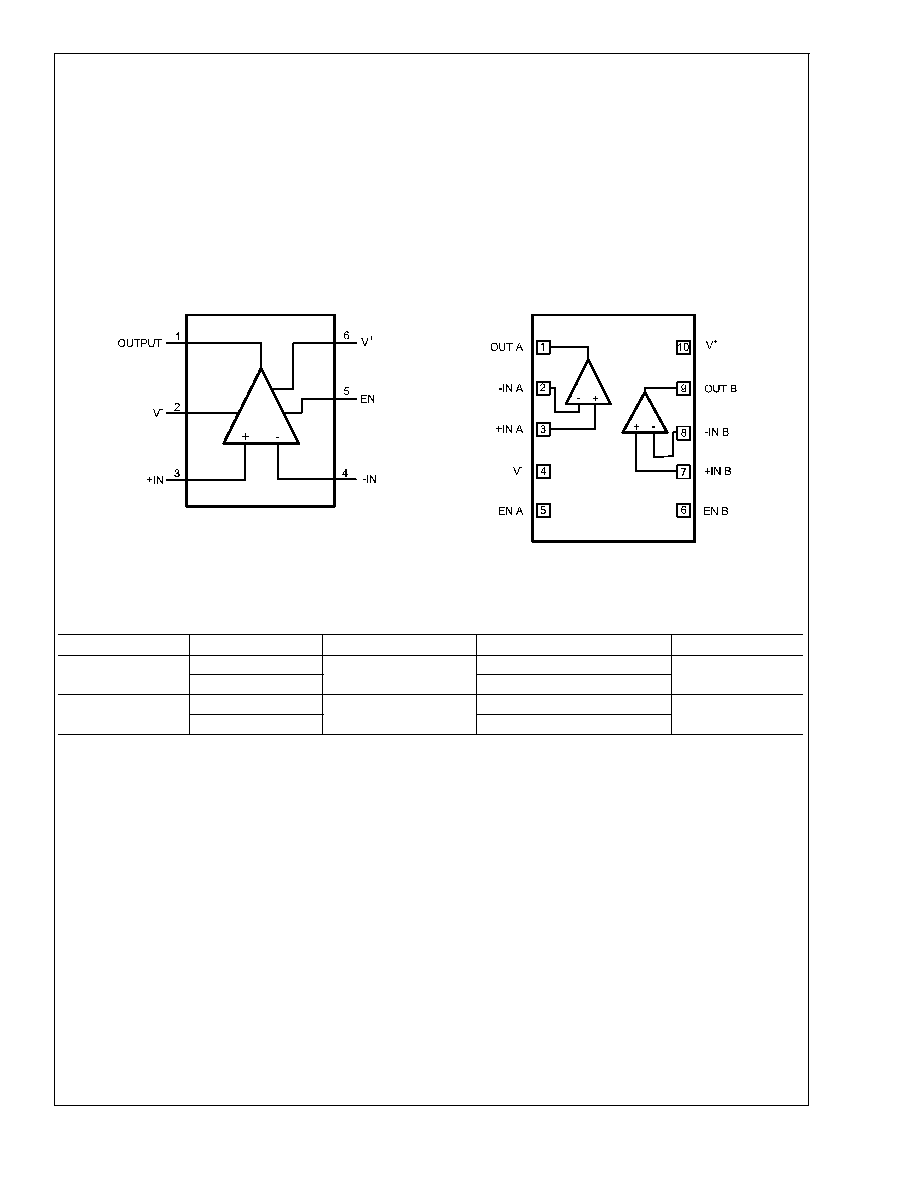
Connection Diagrams
6-Pin TSOT23
10-Pin MSOP
20150301
Top View
20150302
Top View
Ordering Information
Package
Part Number
Package Marking
Transport Media
NSC Drawing
6-Pin TSOT23
LMP7711MK
AC3A
1k Units Tape and Reel
MK06A
LMP7711MKX
3k Units Tape and Reel
10-Pin MSOP
LMP7712MM
AD3A
1k Units Tape and Reel
MUB10A
LMP7712MMX
3.5k Units Tape and Reel
LMP771
1/LMP7712
www.national.com
5