Äîêóìåíòàöèÿ è îïèñàíèÿ www.docs.chipfind.ru
LMH6704
650 MHz Progammable Gain Buffer with Disable
General Description
The LMH
TM
6704 is a very wideband, DC coupled progam-
mable gain buffer designed specifically for wide dynamic
range systems requiring exceptional signal fidelity. The
LMH6704 includes on chip feedback and gain set resistors,
simplifying PCB layout while providing user programmable
gains of +1, +2 and -1 V/V. The LMH6704 provides a disable
pin, which places the amplifier in a high output impedance,
low power mode. The Disable pin may be allowed to float
high.
With a 650 MHz Small Signal Bandwidth (A
V
= +1), full
power gain flatness to 200 MHz, and excellent Differential
Gain and Phase, the LMH6704 is optimized for video appli-
cations. High resolution video systems will benefit from the
LMH6704's ability to drive multiple video loads at low levels
of differential gain or differential phase distortion.
The LMH6704 is constructed with National's proprietary high
speed complementary bipolar process using National's
proven current feedback circuit architectures. It is available
in 8-Pin SOIC and 6-Pin SOT23 packages.
Features
n
Wideband operation
-- A
V
= +1, V
O
= 0.5 V
PP
650 MHz
-- A
V
= +2, V
O
= 0.5 V
PP
450 MHz
-- A
V
= +2, V
O
= 2 V
PP
400 MHz
n
High output current
±
90 mA
n
Very low distortion
-- 2
nd
/3
rd
harmonics (10 MHz, R
L
= 100
):
-62/-78
-- Differential gain/Differential phase:
0.02%/0.02°
n
Low noise
2.3nV/
n
High slew rate
3000 V/µs
n
Supply current
11.5 mA
Applications
n
HDTV, NTSC & PAL video systems
n
Video switching and distribution
n
ADC driver
n
DAC buffer
n
RGB driver
n
High speed multiplexer
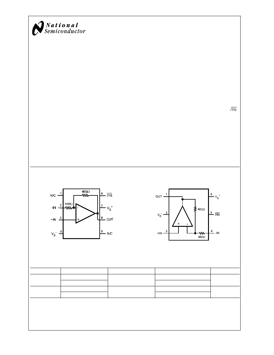
Connection Diagram
8-Pin SOIC
6-Pin SOT23
20103634
Top View
20103613
Top View
Ordering Information
Package
Part Number
Package Marking
Transport Media
NSC Drawing
8-Pin SOIC
LMH6704MA
LMH6704MA
95 Units Rail
M08A
LMH6704MAX
2.5k Units Tape and Reel
6-Pin SOT23
LMH6704MF
B07A
1k Units Tape and Reel
MF06A
LMH6704MFX
3k Units Tape and Reel
LMH
TM
is a trademark of National Semiconductor Corporation.
February 2005
LMH6704
650
MHz
Progammable
Gain
Buffer
with
Disable
© 2005 National Semiconductor Corporation
DS201036
www.national.com
Absolute Maximum Ratings
(Note 1)
If Military/Aerospace specified devices are required,
please contact the National Semiconductor Sales Office/
Distributors for availability and specifications.
Supply Voltage
13.5V
I
OUT
(Note 3)
Common-Mode Input Voltage
V
S
-
to V
S
+
Maximum Junction Temperature
150°C
Storage Temperature Range
-65°C to 150°C
Soldering Information
Infrared or Convection (20 sec.)
235°C
Wave Soldering (10 sec.)
260°C
Lead Temp. (soldering 10 sec.)
300°C
ESD Tolerance (Note 4)
Human Body Model
2000V
Machine Model
200V
Operating Ratings
(Note 1)
Nominal Supply Voltage
±
4V to
±
6V
Operating Temperature
-40°C to 85°C
Thermal Resistance
Package
(
JC
)
(
JA
)
8-Pin SOIC
75°C/W
160°C/W
6-Pin SOT23
120°C/W
187°C/W
Electrical Characteristics
(Note 2)
T
A
= +25°C , A
V
= +2, V
S
=
±
5V, R
L
= 100
; unless specified.
Symbol
Parameter
Conditions
Min
(Note 6)
Typ
(Note 6)
Max
(Note 6)
Units
Dynamic Performance
SSBW
-3 dB Bandwidth
V
OUT
= 0.5 V
PP
, A
V
= +1
650
MHz
SSBW
V
OUT
= 0.5 V
PP
450
LSBW
V
OUT
= 2 V
PP
400
GF
0.1dB
0.1 dB Gain Bandwidth
V
OUT
= 2 V
PP
200
MHz
SR
Slew Rate
V
OUT
= 4 V
PP
, 40% to 60% (Note 5)
3000
V/µs
TRS/TRL
Rise and Fall Time
(10% to 90%)
2V Step
0.9
ns
t
s
Settling Time to 0.1%
2V Step
10
ns
Distortion and Noise Response
HD2L
2
nd
Harmonic Distortion
V
OUT
= 2.0 V
PP
, f = 10 MHz
-62
dBc
HD2H
V
OUT
= 2.0 V
PP
, f = 40 MHz
-52
HD3L
3
rd
Harmonic Distortion
V
OUT
= 2.0 V
PP
, f = 10 MHz
-78
dBc
HD3H
V
OUT
= 2.0 V
PP
, f = 40 MHz
-65
IMD
Two-Tone Intermodulation
f = 10 MHz, P
OUT
= 10 dBm/tone
-65
dBc
V
N
Output Noise Voltage
f = 100 kHz
A
V
= +2
10.5
nV/
A
V
= +1
9.3
A
V
= -1
10.5
I
NN
Non-Inverting Input Noise
Current
3
pA/
DG
Differential Gain
R
L
= 150
, f = 4.43 MHz
.02
%
DP
Differential Phase
R
L
= 150
, f = 4.43 MHz
0.02
deg
Static, DC Performance
A
V
Gain
1.98
1.96
2.00
2.02
2.04
V/V
Gain Error
-1
-2
+1
+2
%
V
IO
Input Offset Voltage
2
±
7
±
8.3
mV
DV
IO
Input Offset Voltage Average
Drift
35
µV/°C
I
BN
Input Bias Current
Non-Inverting (Note 7)
-5
±
15
±
18
µA
I
BI
Input Bias Current
Inverting
5
±
22
±
31
LMH6704
www.national.com
2
Electrical Characteristics
(Note 2) (Continued)
T
A
= +25°C , A
V
= +2, V
S
=
±
5V, R
L
= 100
; unless specified.
Symbol
Parameter
Conditions
Min
(Note 6)
Typ
(Note 6)
Max
(Note 6)
Units
CMIR
Common Mode Input Range
V
IO
15 mV
±
1.9
±
2
V
PSRR
Power Supply Rejection Ratio
DC
48
47
52
dB
V
O
Output Voltage Swing
R
L
=
±
3.3
±
3.18
±
3.5
V
R
L
= 100
±
3.2
±
3.12
±
3.5
I
O
Linear Output Current
V
OUT
80 mV
±
55
±
90
mA
I
S
Supply Current (Enabled)
DIS = 2V, R
L
=
11.5
12.5
13.7
mA
Supply Current (Disabled)
DIS = 0.8V, R
L
=
0.25
0.9
0.925
R
F
& R
G
Internal R
F
and R
G
375
465
563
R
OUT
Closed Loop Output Resistance
DC
0.05
R
IN+
Input Resistance
1
M
C
IN+
Input Capacitance
1
pF
Enable/Disable Performance (Disabled Low)
T
ON
Enable Time
10
ns
T
OFF
Disable Time
10
ns
Output Glitch
50
mV
PP
V
IH
Enable Voltage
DIS
V
IH
2.0
V
V
IL
Disable Voltage
DIS
V
IL
0.8
I
IH
Disable Input Bias Current, High
DIS = V
+
, (Note 7)
-1
±
50
µA
I
IL
Disable Input Bias Current, Low
DIS = 0V (Note 7)
0
-100
-350
µA
I
OZ
Disabled Output Leakage
Current
A
V
= +1, V
OUT
=
±
1.8V
0.2
±
25
±
50
µA
Note 1: Absolute Maximum Ratings indicate limits beyond which damage to the device may occur. Operating Ratings indicate conditions for which the device is
intended to be functional, but specific performance is not guaranteed. For guaranteed specifications, see the Electrical Characteristics tables.
Note 2: Electrical Table values apply only for factory testing conditions at the temperature indicated. Factory testing conditions result in very limited self-heating of
the device such that T
J
= T
A
. No guarantee of parametric performance is indicated in the electrical tables under conditions of internal self-heating where T
J
>
T
A
.
Min/Max ratings are based on production testing unless otherwise specified.
Note 3: The maximum output current (I
OUT
) is determined by device power dissipation limitations.
Note 4: Human body model: 1.5 k
in series with 100 pF. Machine model: 0 in series with 200 pF.
Note 5: Slew Rate is the average of the rising and falling edges.
Note 6: Typical numbers are the most likely parametric norm. Bold numbers refer to over temperature limits.
Note 7: Negative current implies current flowing out of the device.
LMH6704
www.national.com
3
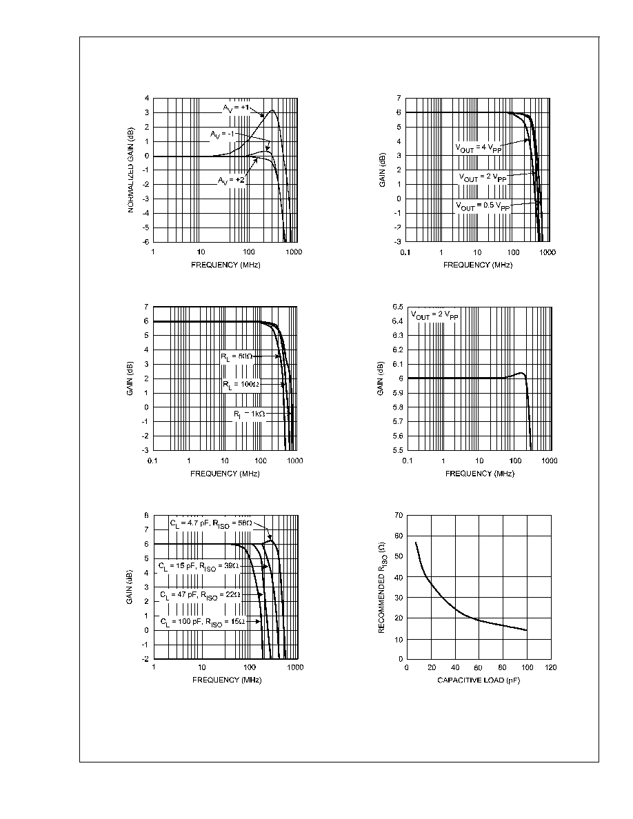
Typical Performance Characteristics
(T
A
= 25°C, V
S
=
±
5V, R
L
= 100
, A
V
= +2, V
OUT
= 0.5 V
PP
;
Unless Specified).
Small Signal Frequency Response vs. Gain
Frequency Response vs. V
OUT
20103614
20103615
Small Signal Frequency Response vs. R
LOAD
Large Signal Gain Flatness
20103616
20103617
Small Signal Frequency Response vs. Capacitive Load
Series Output Isolation Resistance vs. Capacitive Load
20103618
20103619
LMH6704
www.national.com
4
Typical Performance Characteristics
(T
A
= 25°C, V
S
=
±
5V, R
L
= 100
, A
V
= +2, V
OUT
= 0.5 V
PP
;
Unless Specified). (Continued)
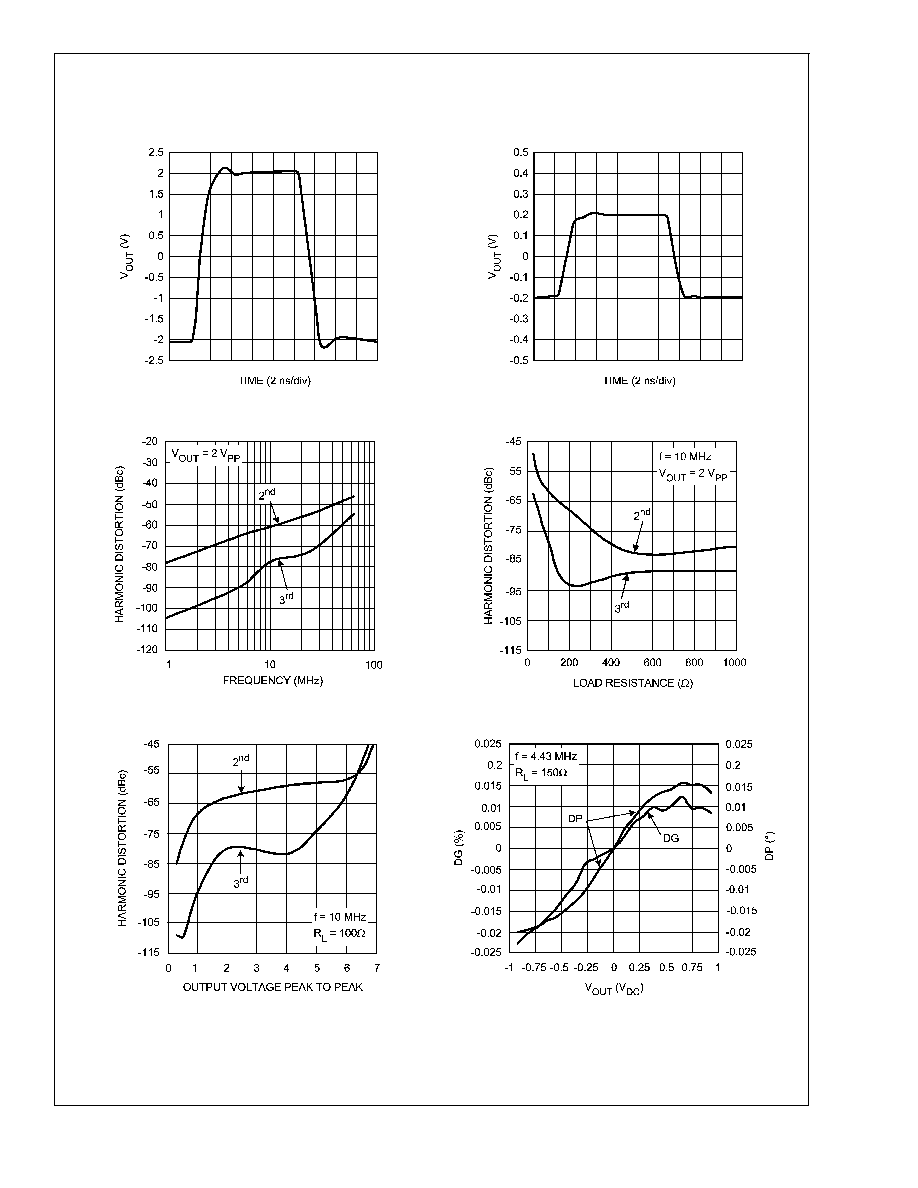
Large Signal Pulse Response
Small Signal Pulse Response
20103620
20103621
Harmonic Distortion vs. Frequency
Harmonic Distortion vs. Load
20103622
20103623
Harmonic Distortion vs. Output Voltage
DG/DP
20103624
20103633
LMH6704
www.national.com
5
Document Outline