TL H 11123
LMF380
Triple
One-Third
Octave
Switched-Capacitor
Active
Filter
November 1995
LMF380 Triple One-Third Octave
Switched-Capacitor Active Filter
General Description
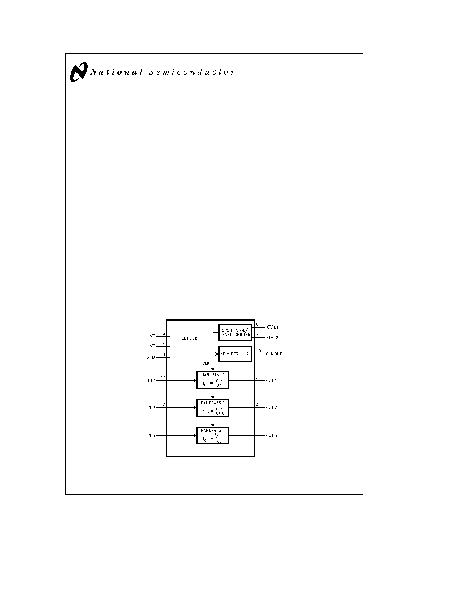
The LMF380 is a triple one-third octave filter set designed
for use in audio audiological and acoustical test and mea-
surement applications Built using advanced switched-ca-
pacitor techniques the LMF380 contains three filters each
having a bandwidth equal to one-third of an octave in fre-
quency By combining several LMF380s each covering a
frequency range of one octave a filter set can be imple-
mented that encompasses the entire audio frequency range
while using only a small fraction of the number of compo-
nents and circuit board area that would be required if a con-
ventional active filter approach were used The center fre-
quency range is not limited to the audio band however
Center frequencies as low as 0 125 Hz or as high as 25 kHz
are attainable with the LMF380
The center frequency of each filter is determined by the
clock frequency The clock signal can be supplied by an
external source or it can be generated by the internal oscil-
lator using an external crystal and two capacitors Since the
LMF380 has an internal clock frequency divider (
d
2) and
an output pin for the half-frequency clock signal a single
clock oscillator for the top-octave LMF380 becomes the
master clock for the entire array of filters in a multiple
LMF380 application
Accuracy is enhanced by close matching of the internal
components the ratio of the clock frequency to the center
frequency is typically accurate to
g
0 5% and passband
gain and stopband attenuation are guaranteed over the full
temperature range
Features
Y
Three bandpass filters with one-third octave center fre-
quency spacing
Y
Choice of internal or external clock
Y
No external components other than clock or crystal and
two capacitors
Key Specifications
Y
Passband gain accuracy Better than 0 7 dB over
temperature
Y
Supply voltage range
g
2V to
g
7 5V or
a
4V to
a
14V
Applications
Y
Real-Time Audio Analyzers (ANSI Type E Class II)
Y
Acoustical Instrumentation
Y
Noise Testing
Simplified Block Diagram
TL H 11123 Ł 1
C1995 National Semiconductor Corporation
RRD-B30M115 Printed in U S A
Absolute Maximum Ratings
(Notes 1
2)
If Military Aerospace specified devices are required
please contact the National Semiconductor Sales
Office Distributors for availability and specifications
Total Supply Voltage
b
0 3V to
a
16V
Voltage at Any Pin
V
b
b
0 3V to V
a
a
0 3V
Input Current per Pin (Note 3)
g
5 mA
Total Input Current (Note 3)
g
20 mA
Lead Temperature (Soldering 10 sec )
Dual-In-Line Package (Plastic)
300 C
Surface Mount Package (Note 4)
Vapor Phase (60 seconds)
215 C
Infrared (15 seconds)
220 C
Power Dissipation (Note 5)
500 mW
Maximum Junction Temperature
150 C
Storage Temperature Range
b
65 C to
a
150 C
ESD Susceptibility (Note 6)
2000V
Operating Ratings
(Note 1)
Temperature Range
T
MIN
s
T
A
s
T
MAX
LMF380CIN LMF380CIV
LMF380CIJ
b
40 C
s
T
A
s
a
85 C
LMF380CMJ
b
55 C
s
T
A
s
a
125 C
Supply Voltage (V
a
b
V
b
)
4 0V to 14V
Clock Input Frequency
10 Hz to 1 25 MHz
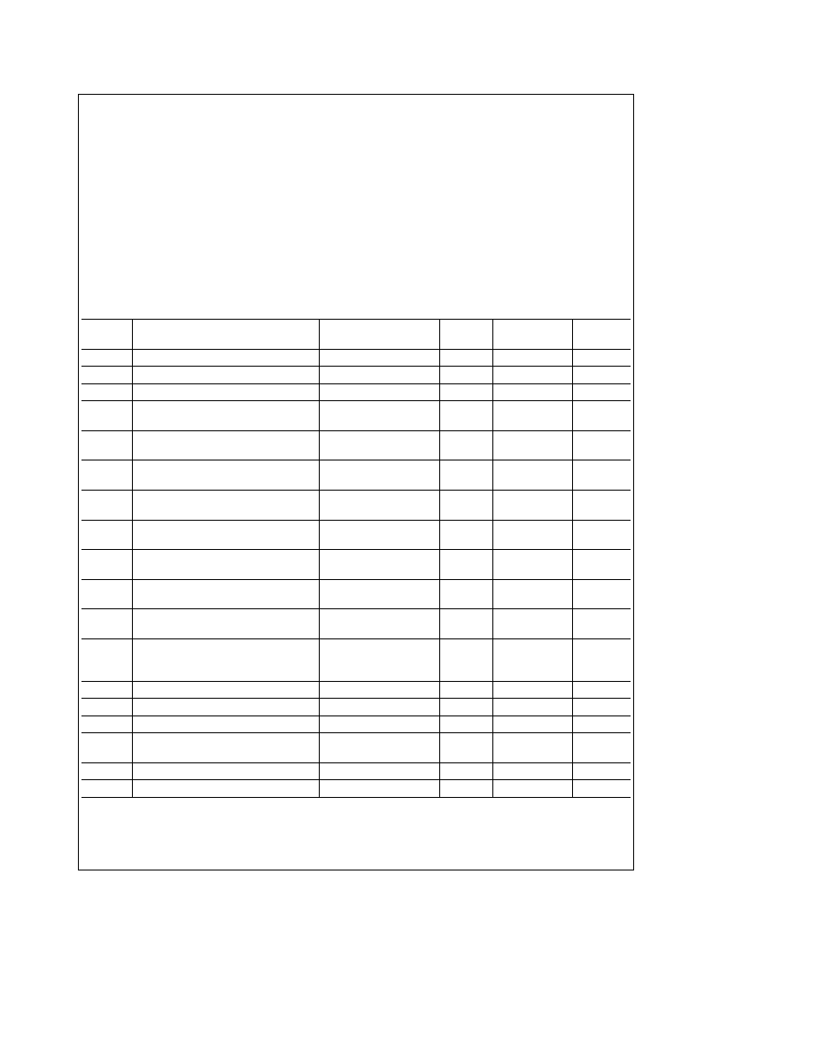
Filter Electrical Characteristics
The following specifications apply for V
a
e a
5V V
b
e b
5V and f
CLK
e
320 kHz unless otherwise specified Boldface limits apply for T
MIN
to T
MAX
all other limits apply for T
A
e
T
J
e
25 C
Symbol
Parameter
Conditions
Typical
Limit
Units
(Note 7)
(Note 8)
(Limit)
f
CLK f01
Clock-to-Center-Frequency Ratio Filter 1
50 1
f
CLK f02
Clock-to-Center-Frequency Ratio Filter 2
62 5 1
f
CLK f03
Clock-to-Center-Frequency Ratio Filter 3
80 1
A
1
Gain at f
1
e
3720 Hz (Filter 1)
(Note 9)
b
32
b
30
dB (max)
2960 Hz (Filter 2) 2340 Hz (Filter 3)
A
2
Gain at f
2
e
6080 Hz (Filter 1)
(Note 9)
a
0 1
0 1
g
0 7
dB (max)
4820 Hz (Filter 2) 3820 Hz (Filter 3)
A
3
Gain at f
3
e
6200 Hz (Filter 1)
(Note 9
0 0
b
0 0
g
0 7
dB (max)
4960 Hz (Filter 2) 3940 Hz (Filter 3)
A
4
Gain at f
4
e
6400 Hz (Filter 1)
(Note 9)
b
0 2
b
0 2
g
0 7
dB (max)
5080 Hz (Filter 2) 4040 Hz (Filter 3)
A
5
Gain at f
5
e
6540 Hz (Filter 1)
(Note 9)
b
0 1
b
0 1
g
0 7
dB (max)
5180 Hz (Filter 2) 4120 Hz (Filter 3)
A
6
Gain at f
6
e
6720 Hz (Filter 1)
(Note 9)
a
0 15
b
0 15
g
0 7
dB (max)
5340 Hz (Filter 2) 4240 Hz (Filter 3)
A
7
Gain at f
7
e
8900 Hz (Filter 1)
(Note 9)
b
22
b
20
dB (max)
7060 Hz (Filter 2) 5600 Hz (Filter 3)
V
OS
Output Offset Voltage Each Filter
a
50
a
120
mV (max)
b
30
mV (min)
En
Total Output Noise OUT1
0 1 Hz to 20 kHz
240
Total Output Noise OUT2
210
m
Vrms
Total Output Noise OUT3
190
C
L
Maximum Capacitive Load
200
pF
Crosstalk
V
IN
e
1 Vrms f
e
f
O
b
67
dB
Clock Feedthrough Each Filter
V
a
e a
5V V
b
e b
5V
10
mV
p-p
V
OUT
Output Voltage Swing
R
L
e
5 kX
a
4 2
a
3 8
V (min)
b
4 6
b
4 2
V (max)
THD
Total Harmonic Distortion
V
IN
e
1 Vrms f
e
f
O
0 05
%
I
S
Supply Current
6 0
9 0
mA (max)
2
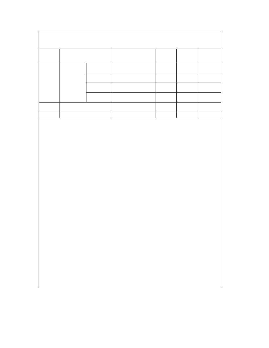
Logic Input and Output Electrical Characteristics
The following specifications for V
a
e a
5V and V
b
e b
5V unless otherwise specified Boldface limits apply for T
MIN
to
T
MAX
all other limits apply for T
A
e
T
J
e a
25 C
Symbol
Parameter
Conditions
(Note 7)
Typical
Tested
(Limit)
Units
Limit
(Note 8)
V
IH
XTAL1
Logical ``1''
V
a
e
5V V
b
e b
5V
a
3 0
V (min)
V
IL
CMOS Clock
Logical ``0''
b
3 0
V (max)
V
IH
Input Voltage
Logical ``1''
V
a
e
10V V
b
e
0V
a
8 0
V (min)
V
IL
Logical ``0''
a
2 0
V (max)
V
IH
Logical ``1''
V
a
e
2 5V V
b
e b
2 5V
a
1 5
V (min)
V
IL
Logical ``0''
b
1 5
V (max)
V
IH
Logical ``1''
V
a
e
5V V
b
e
0V
a
4 0
V (min)
V
IL
Logical ``0''
a
1 0
V (max)
V
OH
Clock Output Logical ``1''
I
OUT
e b
1 mA
V
a
b
1 0
V (min)
V
OL
Clock Output Logical ``0''
I
OUT
e a
1 mA
V
b
a
1 0
V (max)
I
IN
Input Current XTAL1
g
20
m
A (max)
Note 1
Absolute Maximum Ratings indicate limits beyond which damage to the device may occur Operating Ratings indicate conditions for which the device is
functional These ratings do not guarantee specific performance limits however For guaranteed specifications and test conditions see the Electrical Characteris-
tics The guaranteed specifications apply only for the test conditions listed Some performance characteristics may degrade when the device is not operated under
the listed test conditions
Note 2
All voltages are measured with respect to GND unless otherwise specified
Note 3
When the input voltage (V
IN
) at any pin exceeds the power supplies (V
IN
k
V
b
or V
IN
l
V
a
) the current at that pin should be limited to 5 mA The 20 mA
maximum package input current rating limits the number of pins that can safely exceed the power supplies with an input current of 5 mA to four
Note 4
See AN450 ``Surface Mounting Methods and Their Effect on Product Reliability'' or the section titled ``Surface Mount'' found in any volume of the Linear
Data Book Rev 1 for other methods of soldering surface mount devices
Note 5
The maximum power dissipation must be derated at elevated temperatures and is a function of T
Jmax
i
JA
and the ambient temperature T
A
The
maximum allowable power dissipation at any temperature is P
D
e
(T
Jmax
b
T
A
) i
JA
or the number given in the Absolute Maximum Ratings whichever is lower
For guaranteed operation T
Jmax
e
125 C The typical thermal resistance (i
JA
) of the LMF380N when board-mounted is 51 C W i
JA
is typically 52 C W for the
LMF380J and 86 C W for the LMF380V
Note 6
Human body model 100 pF discharged through a 1 5 kX resistor
Note 7
Typicals are at T
J
e
25 C and represent the most likely parametric norm
Note 8
Limits are guaranteed to National's Averge Outgoing Quality Level (AOQL)
Note 9
The nominal test frequencies are f
1
e
0 58 f
O
f
2
e
0 95 f
O
f
3
e
0 98 f
O
f
4
e
f
O
f
5
e
1 02 f
O
f
6
e
1 05 f
O
and f
7
e
1 39 f
O
The actual test
frequencies listed in the table may differ slightly from the nominal values
3
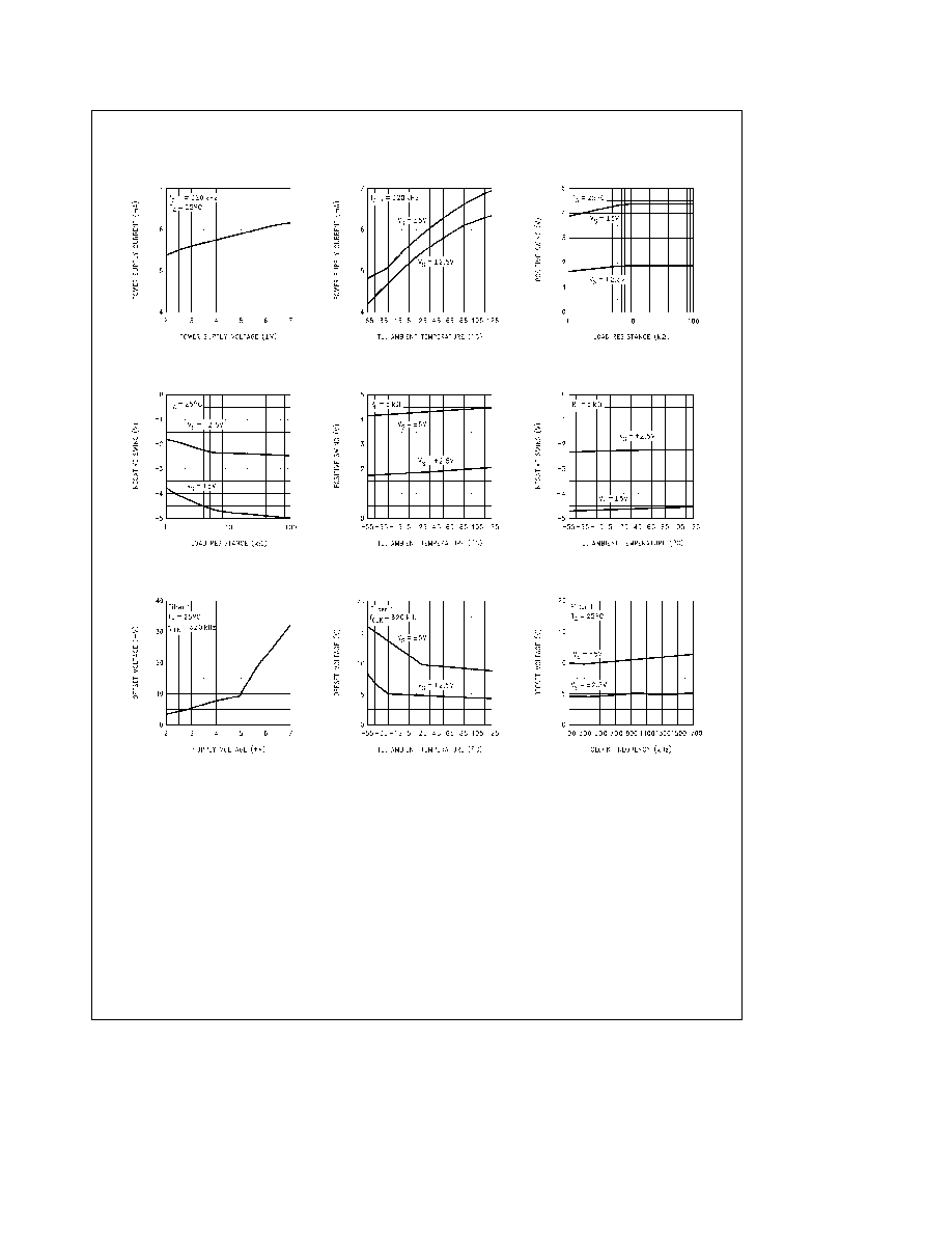
Typical Performance Characteristics
vs Power Supply Voltage
Power Supply Current
vs Temperature
Power Supply Current
vs Load Resistance
Positive Output Swing
vs Load Resistance
Negative Output Swing
vs Temperature
Positive Output Swing
vs Temperature
Negative Output Swing
vs Supply Voltage
Offset Voltage
vs Temperature
Offset Voltage
vs Clock Frequency
Offset Voltage
TL H 11123 Ł 4
4
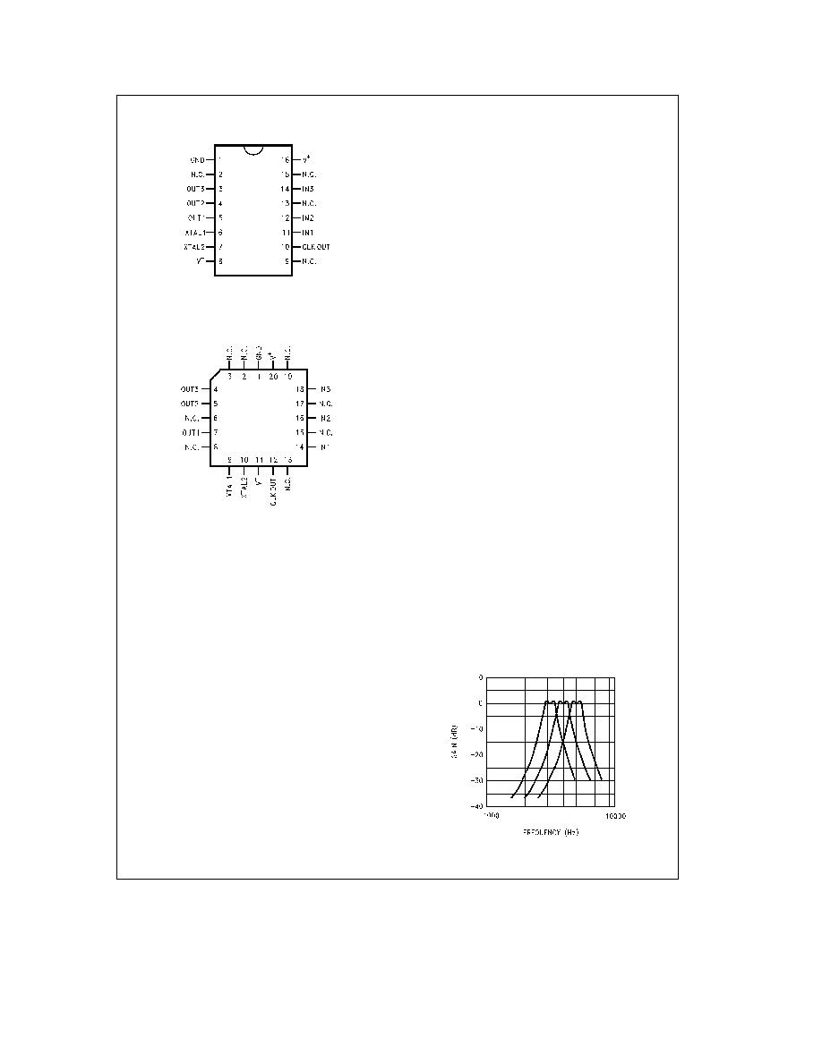
Connection Diagrams
Dual-In-Line Package
TL H 11123 Ł 2
Top View
Order Number LMF380CIJ LMF380CMJ or LMF380CIN
See NS Package Number J16A or N16E
Plastic Chip Carrier Package
TL H 11123 Ł 3
Top View
Order Number LMF380CIV
See NS Package Number V20A
Pin Description
GND
This is the analog ground reference for the
LMF380 In split supply applications GND
should be connected to the system ground
When operating the LMF380 from a single
positive power supply voltage pin 1 should
be connected to a ``clean'' reference volt-
age midway between V
a
and V
b
N C
These pins are not connected to the inter-
nal circuitry
OUT1 OUT2
These are the outputs of the filters
OUT3
XTAL1
This is the crystal oscillator input pin When
using the internal oscillator
the crystal
should be tied between XTAL1 and XTAL2
XTAL1 also serves as the input for an exter-
nal CMOS-level clock
XTAL2
This is the output of the internal crystal
oscillator When using the internal oscilla-
tor the crystal should be tied between
XTAL1 and XTAL2
V
b
This is the negative power supply pin It
should be bypassed with at least a 0 1 mF
ceramic capacitor
For best results
a
1 0 mF to 10 0 mF tantalum capacitor
should also be used For single-supply op-
eration connect this pin to system ground
CLOCK OUT
This is the clock output pin It can drive the
clock inputs (XTAL1) of additional LMF380s
or other components The clock output fre-
quency is one-half the clock frequency at
XTAL1
INPUT1
These are the signal inputs to the filters
INPUT2
INPUT3
V
a
This is the positive power supply pin It
should be bypassed with at least a 0 1 mF
ceramic capacitor For best results a 1 0
m
F to 10 0 mF tantalum capacitor should
also be used
Functional Description
The LMF380 contains three fourth-order Chebyshev band-
pass filters whose center frequencies are spaced one-third
of an octave apart making it ideal for use in ``real time''
audio spectrum analysis applications
As with other
switched-capacitor filters the center frequencies are pro-
portional to the clock frequency applied to the IC the center
frequencies of the LMF380's three filters are located at
f
CLK
50 f
CLK
62 5 and f
CLK
80
The three filters in an LMF380 cover a full octave in fre-
quency so that by using several LMF380s with clock fre-
quencies separated by a factor of 2n a complex audio pro-
gram can be analyzed for frequency content over a range of
several octaves To facilitate this the CLK OUT pin of the
LMF380 supplies an output clock signal whose frequency is
one-half that of the incoming clock frequency Therefore a
single clock source can provide the clock reference for all of
the 30 filters (10LMF380s) in a real time analyzer that cov-
ers the entire 10-octave audio frequency range
The
LMF380 contains an internal clock oscillator that requires
an external crystal and two capacitors to operate Since the
clock divider is on-board only a single crystal is needed for
the top-octave filter chip the remaining devices can derive
their clock signals from the master If desired an external
oscillator can be used instead
Figure 1 shows the magnitude versus frequency curves for
the three filters in the LMF380 Separate input and output
pins are provided for the three internal filters The input pins
will normally be connected to a common signal source but
can also be connected to separate input signals when nec-
essary
TL H 11123 Ł 6
FIGURE 1 Response curves for the three filters in the
LMF380 The clock frequency is 250 kHz
5