TL H 5176
LM832
Dynamic
Noise
Reduction
System
DNR
August 1989
LM832 Dynamic Noise Reduction System DNR
General Description
The LM832 is a stereo noise reduction circuit for use with
audio playback systems The DNR system is noncomple-
mentary meaning it does not require encoded source mate-
rial The system is compatible with virtually all prerecorded
tapes and FM broadcasts Psychoacoustic masking and an
adaptive bandwidth scheme allow the DNR to achieve 10
dB of noise reduction DNR can save circuit board space
and cost because of the few additional components re-
quired
The LM832 is optimized for low voltage operation with input
levels around 30 mVrms
For higher input levels use the LM1894
DNR
is a registered trademark of National Semiconductor Corporation
The DNR
system is licensed to National Semiconductor Corp under U S patent 3 678 416
and 3 753 159
A trademark and licensing agreement is required for the use of this product
Features
Y
Low voltage battery operation
Y
Non-complementary noise reduction ``single ended''
Y
Low cost external components no critical matching
Y
Compatible with all prerecorded tapes and FM
Y
10 dB effective tape noise reduction CCIR ARM
weighted
Y
Wide supply range 1 5V to 9V
Y
150 mVrms input overload
Y
No royalty requirements
Y
Cascade connection for 17 dB noise reduction
Applications
Y
Headphone stereo
Y
Microcassette players
Y
Radio cassette players
Y
Automotive radio tape players
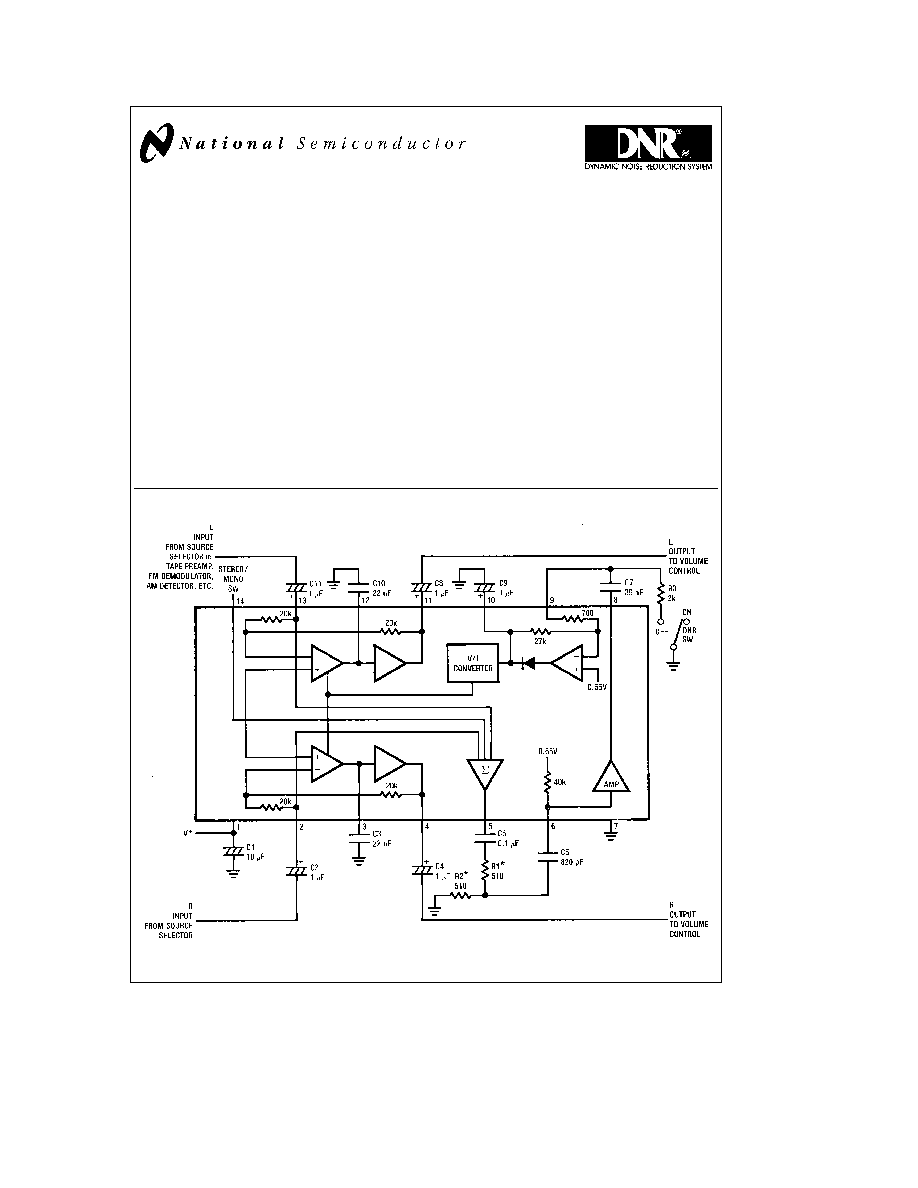
Application Circuit
Order Number LM832M See NS Package M14A
Order Number LM832N See NS Package N14A
TL H 5176 Ł 1
FIGURE 1 Component Hook-up for Stereo DNR System
C1995 National Semiconductor Corporation
RRD-B30M115 Printed in U S A
Absolute Maximum Ratings
If Military Aerospace specified devices are required
please contact the National Semiconductor Sales
Office Distributors for availability and specifications
Supply Voltage
10V
Power Dissipation (Note 1)
1 2W
Input Voltage
1 7 Vpp
Storage Temperature
b
65 to
a
150 C
Operating Temperature (Note 1)
b
40 to
a
85
Soldering Information
Y
Dual-In-Line Package
Soldering (10 seconds)
260 C
Y
Small Outline Package
Vapor Phase (60 seconds)
215 C
Infrared (15 seconds)
220 C
See AN-450 ``Surface Mounting Methods and Their Effects
on Products Reliability'' for other methods of soldering sur-
face mount devices ''
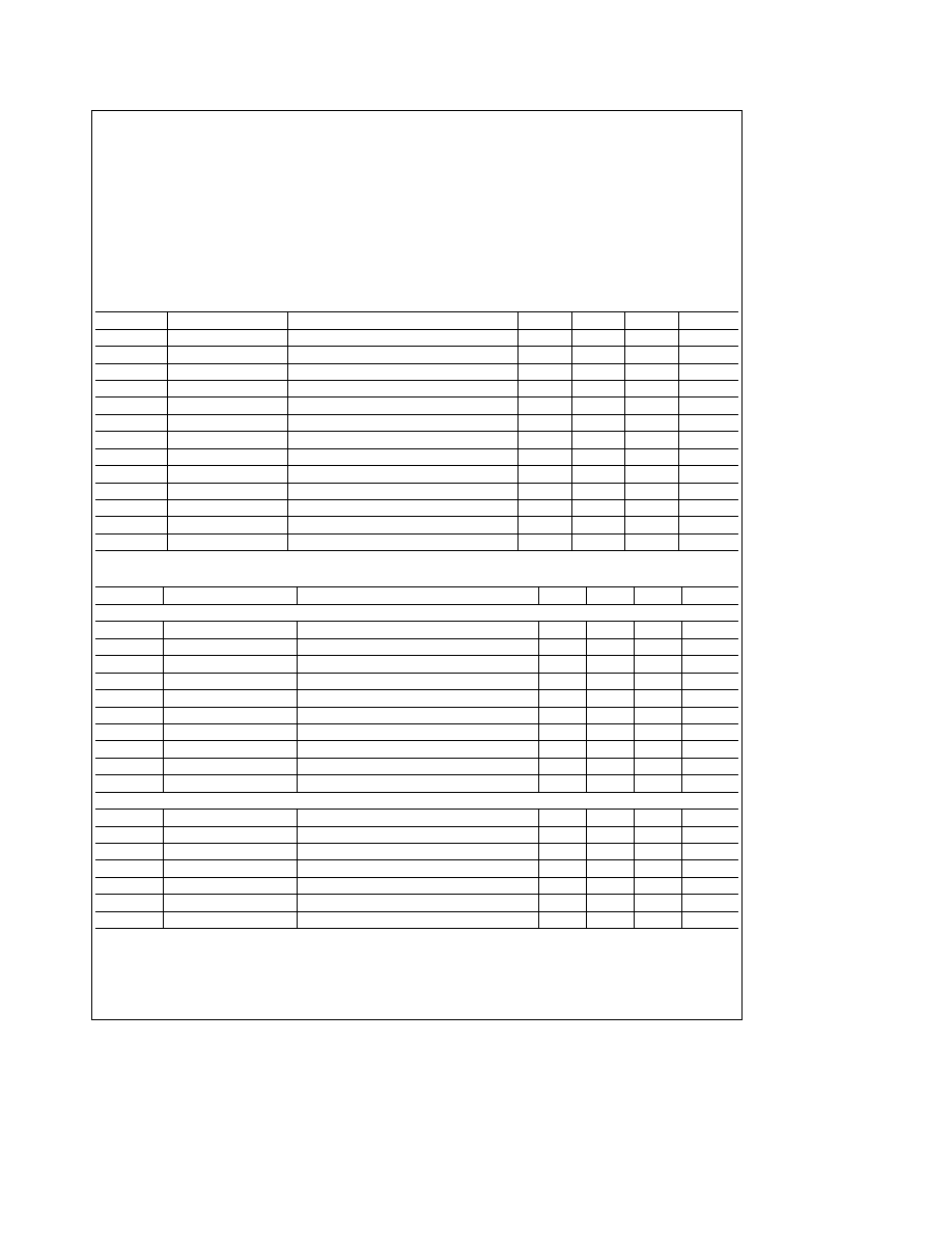
DC Electrical Characteristics
T
A
e
25 C V
CC
e
3 0V
Symbol
Parameter
Conditions
Min
Typ
Max
Units
V
OP
Operating Voltage
Supply Voltage for Normal Operation
1 5
3 0
9 0
V
I
CC
(1)
Supply Current (1)
Pin 9 to GND 0 1 mF BW
e
Min Note 2
2 5
4 0
mA
I
CC
(2)
Supply Current (2)
DC GND Pin 9 with 2k BW
e
Max Note 2
5 0
8 0
mA
V
IN
(1)
Input Voltage (1)
Pin 2 Pin 13
0 20
0 36
0 5
V
V
IN
(2)
Input Voltage (2)
Pin 6
0 50
0 65
0 8
V
V
IN
(3)
Input Voltage (3)
Pin 9
0 50
0 65
0 8
V
V
OUT
(1)
Output Voltage (1)
Pin 4 Pin 11
0 20
0 35
0 50
V
V
OUT
(2)
Output Voltage (2)
Pin 5 Stereo Mode
0 15
0 28
0 40
V
V
OUT
(3)
Output Voltage (3)
Pin 5 Monaural Mode DC Ground Pin 14
0 10
0 20
0 30
V
V
OUT
(4)
Output Voltage (4)
Pin 8
0 25
0 40
0 60
V
V
OUT
(5)
Output Voltage (5)
Pin 10 BW
e
Max Note 2
1 00
1 27
1 50
V
V
OUT
(6)
Output Voltage (6)
Pin 10 BW
e
Min Note 2
0 50
0 65
0 75
V
V
OS
Output DC Shift
Pin 4 PIN 11 Change BW Min to Max
1 0
3 0
mV
AC Electrical Characteristics
Symbol
Parameter
Conditions
Min
Typ
Max
Units
MAIN SIGNAL PATH (Note 3)
A
V
Voltage Gain
V
IN
e
30 mVrms f
e
1 kHz BW
e
Max Note 2
b
1 0
0 0
a
1 0
dB
C B
Channel Balance
V
IN
e
30 mVrms f
e
1 kHz BW
e
Max Note 2
b
1 0
0
a
1 0
dB
f
MIN
Min Bandwidth
0 1 mF between Pin 9 - GND
600
1000
1500
Hz
f
MAX
Max Bandwidth
DC Ground Pin 9 with 2k
24
30
46
kHz
THD
Distortion
V
IN
e
30 mVrms f
e
1 kHz BW
e
Max Note 2
0 07
0 5
%
MV
IN
Max Input Voltage
THD
e
3% f
e
1 kHz BW
e
Max Note 2
120
150
mVrms
S N
Signal to Noise
REF
e
30 mVrms BW
e
Max CCIR ARM
60
68
dB
Z
IN
Input Impedance
Pin 2 Pin 13
14
20
26
kX
C S
Channel Separation
Ref
e
30 mVrms f
e
1 kHz BW
e
Max Note 2
40
68
dB
P
SRR
P
SRR
V
RIPPLE
e
50 mVrms f
e
100 Hz
40
55
dB
CONTROL PATH
A
V
sum(1)
Summing Amp Gain (1)
V
IN
e
30 mVrms at R and L f
e
1 kHz
b
3 0
b
1 5
0 0
dB
A
V
sum(2)
Summing Amp Gain (2)
DC Ground Pin 14 f
e
1 kHz
b
9 0
b
6 0
b
3 0
dB
A
V
1st
Gain Amp Gain
Pin 6 to Pin 8
25
30
35
dB
Z
IN
1st
Input Impedance
Pin 6
28
40
52
kX
A
VPKD
Peak Detector Gain
AC In DC Out Pin 9 to Pin 10
25
30
35
V V
Z
INPKD
Input Impedance
Pin 9
500
800
1100
X
V
RPKD
Output DC Change
Pin 10 Change BW Min to Max
0 5
0 62
0 8
V
Note 1
For operation in ambient temperature above 25 C the device must be derated based on a 150 C maximum junction temperature and a thermal resistance
junction to ambient as follows LM832N
b
90 c w LM832M-115 c w
Note 2
To force the DNR system into maximum bandwidth connect a 2k resistor from pin 9 to GND AC ground pin 9 or pin 6 to select minimum bandwidth To
change minimum and maximum bandwidth see Application Hints
Note 3
The maximum noise reduction CCIR ARM weighted is about 14 dB This is accomplished by changing the bandwidth from maximum to minimum In actual
operation minimum bandwidth is not selected a nominal minimum bandwidth of about 2 kHz gives 10 dB of noise reduction See Application Hints
2

External Component Guide
(See
Figure 1 )
Recom-
Effect
P N
mended
Purpose
Smaller
Larger
Remarks
Value
C1
10 mF
Power supply
Poor supply
Better supply
Do not use less
decoupling
rejection
rejection
than 10 mF
C2 C11
1 mF
Input coupling
Increases
Reduces
DC voltage at pin 2
capacitor
frequency of low-
frequency of low-
and pin 13 is 0 35V
frequency roll-off
frequency roll-off
f
e
1
2
q
C
2
R
IN
C3 C10
22 nF for Stereo
Establishment of Min
Bandwidth
Bandwidth
See Note 4
15 nF for mono
and Max Bandwidth
becomes wider
becomes narrower
C4 C8
1 mF
Output coupling
Increases
Reduces
DC voltage at pin 4
capacitor
frequency of low-
frequency of low-
and pin 11 is 0 35V
frequency roll-off
frequency roll-off
f
e
1
2
q
C
4
R
LOAD
Works with R1 and R2
Some high frequency
Bandwidth may
to set one of the low-
program material
increase due
C5
0 1 mF
frequency corners
may be attenuated
to low-frequency
f
e
1
2
q
C
5
(R1
a
R2)
e
1 6 kHz
in control path
inputs causing
``Breathing''
See Note 4
Works with input
resistance of pin 6
C6
820 pF
to set one of the
Same as
Same as
f
e
1
2
q
C
6
R
PIN6
e
4 8 kHz
low-frequency
above
above
corners in the
See Note 4
control path
Works with input
resistance of pin 9
Same as
Same as
C7
39 nF
to form part of
above
above
f
e
1
2
q
C
7
R
PIN7
e
4 8 kHz
control path
frequency weighing
See Note 4
C9
1 mF
Sets attack time
Reduces attack
Increases attack
See Note 4
and decay time
and decay time
This voltage
Sensitivity should be set for
R1 R2
R
1
a
R
2
e
1 kX
divider sets
maximum noise reduction
control path
and minimum audible
sensitivity
frequency program effect
on high
R3
2 kX
Sets gain amp load
Loads gain amp
Max bandwidth
when DNR is OFF
output may
will be reduced
cause distortion
Note 4
The values of the control path filter components (C5 C6 C7 C9 R1 R2) and the integrating capacitors (C3 C10) should not be changed from the
recommended values unless the characteristics of the noise or program material differ substantially from that of FM or tape sources Failure to use the correct
values may result in degraded performance and therefore the application may not be approved for DNR trademark usage Please contact National Semiconductor
for more information and technical assistance
3
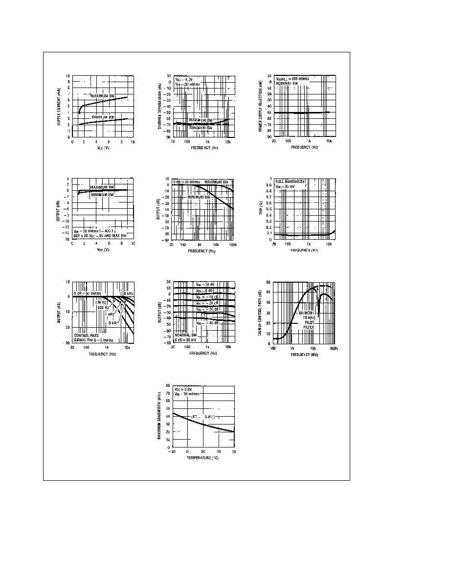
Typical Performance Characteristics
TL H 5176 Ł 2
FIGURE 2 Supply current
vs supply voltage
TL H 5176 Ł 3
FIGURE 3 Channel separation
vs frequency
TL H 5176 Ł 4
FIGURE 4 Power supply
rejection ratio vs frequency
TL H 5176 Ł 5
FIGURE 5 Output level
change vs supply voltage
TL H 5176 Ł 6
FIGURE 6 Output level
vs frequency
TL H 5176 Ł 7
FIGURE 7 THD vs
frequency
TL H 5176 Ł 8
FIGURE 8 Output vs frequency
and control path signal
TL H 5176 Ł 9
FIGURE 9 Frequency response
for various input levels
TL H 5176 Ł 10
FIGURE 10 Gain of control
path vs frequency
TL H 5176 Ł 11
FIGURE 11 Change in main signal path
maximum bandwidth vs temperature
4

Circuit Operation
The LM832 has two signal paths a main signal path and a
bandwidth control path The main path is an audio low pass
filter comprised of a g
m
block with a variable current and a
unity gain buffer As seen in
Figure 1 DC feedback con-
strains the low frequency gain to A
v
e b
1 Above the cutoff
frequency of the filter the output decreases at
b
6 dB oct
due to the action of the 0 022 mF capacitor
The purpose of the control path is to generate a bandwidth
control signal which replicates the ear's sensitivity to noise
in the presence of a tone A single control path is used for
both channels to keep the stereo image from wandering
This is done by adding the right and left channels together
in the summing amplifier of
Figure 1 The R1 R2 resistor
divider adjusts the incoming noise level to slightly open the
bandwidth of the low pass filter Control path gain is about
60dB and is set by the gain amplifier and peak detector
gain This large gain is needed to ensure the low pass filter
bandwidth can be opened by very low noise floors The ca-
pacitors between the summing amplifier output and the
peak detector input determine the frequency weighting as
shown in the typical performance curves The 1 mF capaci-
tor at pin 10 in conjunction with internal resistors sets the
attack and decay times The voltage is converted into a
proportional current which is fed into the g
m
blocks The
bandwidth sensitivity to g
m
current is 70 Hz mA In FM
stereo applications a 19 kHz pilot filter is inserted between
pin 8 and pin 9 as shown in
Figure 16
Normal methods of evaluating the frequency response of
the LM 832 can be misleading if the input signal is also
applied to the control path Since the control path includes a
frequency weighting network a constant amplitude but vary-
ing frequency input signal will change the audio signal path
bandwidth in a non-linear fashion Measurements of the au-
dio signal path frequency response will therefore be in error
since the bandwidth will be changing during the measure-
ment See
Figure 9 for an example of the misleading results
that can be obtained from this measurement approach Al-
though the frequency response is always flat below a single
high-frequency pole the lower curves do not resemble sin-
gle pole responses at all
A more accurate evaluation of the frequency response can
be seen in
Figure 8 In this case the main signal path is
frequency swept while the control path has a constant fre-
quency applied It can be seen that different control path
frequencies each give a distinctive gain roll-off
PSYCHOACOUSTIC BASICS
The dynamic noise reduction system is a low pass filter that
has a variable bandwidth of 1 kHz to 30 kHz dependent on
music spectrum The DNR system operates on three princi-
ples of psychoacoustics
1 Music and speech can mask noise In the absence of
source material background noise can be very audible
However when music or speech is present the human ear
is less able to distinguish the noise
the source material is
said to mask the noise The degree of masking is depen-
dent on the amplitude and spectral content (frequencies) of
the source material but in general multiple tones around 1
kHz are capable of providing excellent masking of noise
over a very wide frequency range
2 The ear cannot detect distortion for less than 1 ms On a
transient basis if distortion occurs in less than 1 ms the ear
acts as an integrator and is unable to detect it Because of
this signals of sufficient energy to mask noise open the
bandwidth to 90% of the maximum value in less than 1 ms
Reducing the bandwidth to within 10% of its minimum value
is done in about 60 ms long enough to allow the ambience
of the music to pass through but not so long as to allow the
noise floor to become audible
3 Reducing the audio bandwidth reduces the audibility of
noise Audibility of noise is dependent on noise spectrum or
how the noise energy is distributed with frequency Depend-
ing on the tape and the recorder equalization tape noise
spectrum may be slightly rolled off with frequency on a per
octave basis The ear sensitivity on the other hand greatly
increases between 2 kHz and 10 kHz Noise in this region is
extremely audible The DNR system low pass filters this
noise Low frequency music will not appreciably open the
DNR bandwidth thus 2 kHz to 20 kHz noise is not heard
Application Hints
The DNR system should always be placed before tone and
volume controls as shown in
Figure 1 This is because any
adjustment of these controls would alter the noise floor
seen by the DNR control path The sensitivity resistors R1
and R2 may need to be switched with the input selector
depending on the noise floors of different sources i e tape
FM phono To determine the value of R1 and R2 in a tape
system for instance apply tape noise (no program material)
and adjust the ratio of R1 and R2 to slightly open the band-
width of the main signal path This can easily be done by
viewing the capacitor voltage of pin 10 with an oscilloscope
or by using the circuit of
Figure 12 This circuit gives an LED
display of the voltage on the peak detector capacitor Adjust
the values of R1 and R2 (their sum is always 1 kX) to light
the LEDs of pin 1 and pin 18 The LED bar graph does not
indicate signal level but rather instantaneous bandwidth of
the two filters it should not be used as a signal-level indica-
tor For greater flexibility in setting the bandwidth sensitivity
R1 and R2 could be replaced by a 1 kX potentiometer
To change the minimum and maximum value of bandwidth
the integrating capacitors C3 and C10 can be scaled up or
down Since the bandwidth is inversely proportional to the
capacitance changing this 0 022 mF capacitor to 0 015 mF
will change the typical bandwidth from 1 kHz Ł 30 kHz to 1 5
kHz Ł 44 kHz With C3 and C10 set at 0 022 mF the maxi-
mum bandwidth is typically 30 kHz A double pole double
throw switch can be used to completely bypass DNR
The capacitor on pin 10 in conjunction with internal resistors
sets the attack and decay times The attack time can be
altered by changing the size of C9 Decay times can be
decreased by paralleling a resistor with C9 and increased
by increasing the value of C9
When measuring the amount of noise reduction of DNR in a
cassette tape system the frequency response of the cas-
sette should be flat to 10 kHz The CCIR weighting network
has substantial gain to 8 kHz and any additional roll-off in
the cassette player will reduce the benefits of DNR noise
reduction A typical signal-to-noise measurement circuit is
shown in
Figure 13 The DNR system should be switched
from maximum bandwidth to nominal bandwidth with tape
noise as a signal source The reduction in measured noise is
the signal-to-noise ratio improvement
5