Äîêóìåíòàöèÿ è îïèñàíèÿ www.docs.chipfind.ru
TL H 12545
LM6310
High
Speed
Low
Power
Operational
Amplifier
with
TRI-STATE
Output
November 1995
LM6310
High Speed Low Power Operational
Amplifier with TRI-STATE
Output
General Description
The LM6310 is a video speed operational amplifier with a
fast easy to use disable function This disable function puts
the amplifier output into a high impedance state This makes
the LM6310 ideal for distributed video multiplexing where
channels can be on different boards This can enhance
manufacturing flexibility by making it easy to add or delete
options to basic designs
The disable function can also be used for half-duplex com-
munication The disable function also reduces power con-
sumption The LM6310 uses a current feedback design for
improved gain flatness making it a good choice for high
quality video designs Operating from
g
5V supplies the
LM6310 is ideal for low power designs
Features
Y
90 MHz
b
3 dB bandwidth
Y
TRI-STATE output disable to high impedance
Y
Disable time
k
25 ns
Y
TTL CMOS compatible disable input
Y
Typical differential gain 0 05%
Y
Typical differential Phase 0 33
Y
60 mA output current
Y
Typical supply current
k
4 5 mA
Y
k
1 mA current when disabled
Y
Specified for
g
5V operation
Applications
Y
Cable TV Set Top Boxes
Y
Video Multiplexers and Multimedia Cards
Y
Virtual Reality and Desktop Video
Y
Portable Video
Y
Video Distribution
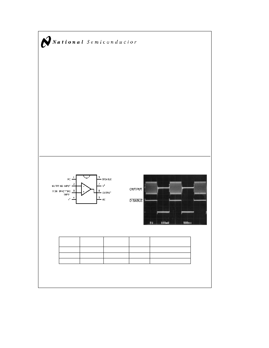
Connection Diagram
8-Pin DIP SO-8
TL H 12545 1
Top View
TL H 12545 2
Package
Ordering
NSC Drawing
Package
Transport Media
Information
Number
Marking
8-Pin DIP
LM6310IN
N08E
LM6310IN
Rails
8-Pin SO-8
LM6310IM
M08A
LM6310IM
Rails
8-Pin SO-8
LM6310IMX
M08A
LM6310IM
2 5k Units Tape and Reel
TRI-STATE
is a registered trademark of National Semiconductor Corporation
TinyPaK
TM
is a trademark of National Semiconductor Corporation
C1996 National Semiconductor Corporation
RRD-B30M66 Printed in U S A
http
www national com
Absolute Maximum Ratings
(Note 1)
If Military Aerospace specified devices are required
please contact the National Semiconductor Sales
Office Distributors for availability and specifications
ESD Tolerance (Note 2)
1500V
Differential Input Voltage
g
2V
Voltage at Input Output Pin
(V
a
)
a
0 1V (V
b
)
b
0 1V
Supply Voltage (V
a
V
b
)
12V
Current at Input Pin
g
5 mA
Current at Output Pin (Note 3)
g
80 mA
Current at Power Supply Pin
80 mA
Lead Temp (soldering 10 sec )
260 C
Storage Temperature Range
b
65 C to
a
150 C
Junction Temperature (Note 4)
150 C
Operating Ratings
(Note 1)
Supply Voltage
V
b
e b
5V V
a
e a
5V
Junction Temperature Range
LM6310I
b
40 C
s
T
J
s
a
85 C
Thermal resistance (i
JA
)
N Package 8-pin Molded DIP
125 C W
SO-8 Package 8-Pin Surface Mount
165 C W
g
5V DC Electrical Characteristics
Unless otherwise specified all limits guaranteed for T
J
e
25 C V
a
e
5V V
b
e b
5V V
CM
e
V
O
e
0V and R
L
e
100X Boldface limits apply at the temperature extremes
Typ
LM6310I
Symbol
Parameter
Conditions
(Note 5)
Limit
Units
(Note 6)
V
OS
Input Offset Voltage
1
5
mV
9
max
TCV
OS
Input Offset Voltage
30
m
V C
Average Drift
I
B
Input Bias Current
0 2
1 5
m
A
Non-Inverting (
a
) Input
3 0
max
I
B
Input Bias Current
2
8
m
A
Inverting (
b
) Input
14
max
R
IN
Input Resistance
6
MX
Non-Inverting (
a
) Input
R
IN
Input Resistance
180
X
Inverting (
b
) Input
CMRR
Common Mode
b
1 0V
s
V
CM
s
a
1 0V
50
43
db
Rejection Ratio
40
min
a
PSRR
Positive Power
V
a
e
4 5V to 5 5V
52
46
db
Supply Rejection Ratio
V
b
e b
5 0V
42
min
b
PSRR
Negative Power
V
a
e
5 0V
52
46
db
Supply Rejection Ratio
V
b
e b
4 5V to
b
5 5V
42
min
C
IN
Common-Mode
2
pF
Input Capacitance
V
O
Output Swing
R
L
e
100X
3 5
3 1
V
2 4
min
b
2 8
b
2 7
V
b
1 6
max
R
L
e
%
4 0
3 9
V
3 7
min
b
3 3
b
3 2
V
b
2 8
max
http
www national com
2
g
5V DC Electrical Characteristics
Unless otherwise specified all limits guaranteed for T
J
e
25 C V
a
e
5V V
b
e b
5V V
CM
e
V
O
e
0V and R
L
e
100X Boldface limits apply at the temperature extremes (Continued)
Typ
LM6310I
Symbol
Parameter
Conditions
(Note 5)
Limit
Units
(Note 6)
I
SC
Output Current
10X to 0V
60
44
mA
Sourcing
20
min
R
OUT
Output Resistance
Closed Loop
0 06
X
max
I
S
Supply Current for
DISABLE (Pin 8)
l
2 0V
3 5
4 5
mA
Normal Operation Mode
5 0
max
I
S
Supply Current Powerdown
DISABLE (Pin 8)
k
0 8V
0 8
1 0
mA
(TRI-STATE) Mode
1 2
max
g
5V AC Electrical Characteristics
Unless otherwise specified all limits guaranteed for T
J
e
25 C V
a
e
5V V
b
e b
5V V
CM
e
V
O
e
0V and R
L
e
100X Boldface limits apply at the temperature extremes
Typ
LM6310I
Symbol
Parameter
Conditions
(Note 5)
Limit
Units
(Note 6)
SR
Slew Rate
A
V
e a
2 2V Output Pulse
300
V ms
b
3 dB BW
b
3db Bandwidth
A
V
e a
2
90
MHz
Dg
Differential Gain
A
V
e a
2 150X Load (75X Back-Terminated)
0 05
%
(Note 7)
1 kX Pull-Down to
b
5V on Output
Dp
Differential Phase
A
V
e a
2 150X Load (75X Back-Terminated)
0 33
(Note 7)
1 kX Pull-Down to
b
5V on Output
e
n
Input-Referred
f
e
1 MHz
5
nV
0
Hz
Voltage Noise
Input-Referred Current Noise
f
e
1 MHz
3
pA
0
Hz
Non-Inverting (
b
) Input
Input-Referred Current
f
e
1 MHz
12
pA
0
Hz
Noise Inverting (
b
) Input
t
ON
Turn On Time
DISABLE (Pin 8) Low to High
50
ns
t
OFF
Turn Off Time
DISABLE (Pin 8) High to Low
25
ns
Output Isolation
Output Isolation from Inputs when
55
db
DISABLE
e
Low 10 MHz
Note 1
Absolute Maximum Ratings indicate limits beyond which damage to the device may occur Operating Ratings indicate conditions for which the device is
intended to be functional but specific performance is not guaranteed For guaranteed specifications and the test conditions see the Electrical characteristics
Note 2
Human body model 1 5 kX in series with 100 pF
Note 3
Applies to both single-supply and split-supply operation Continuous short circuit operation at elevated ambient temperature can result in exceeding the
maximum allowed junction temperature of 150 C
Note 4
The maximum power dissipation is a function of T
J(max)
i
JA
and T
A
The maximum allowable power dissipation at any ambient temperature is P
D
e
(T
J(max)
T
A
) i
JA
All numbers apply for packages soldered directly into a PC board
Note 5
Typical values represent the most likely parametric norm
Note 6
All limits are guaranteed by testing or statistical analysis
Note 7
Differential Gain and Phase performance is sensitive to layout Follow layout suggestions in text for best results
http
www national com
3
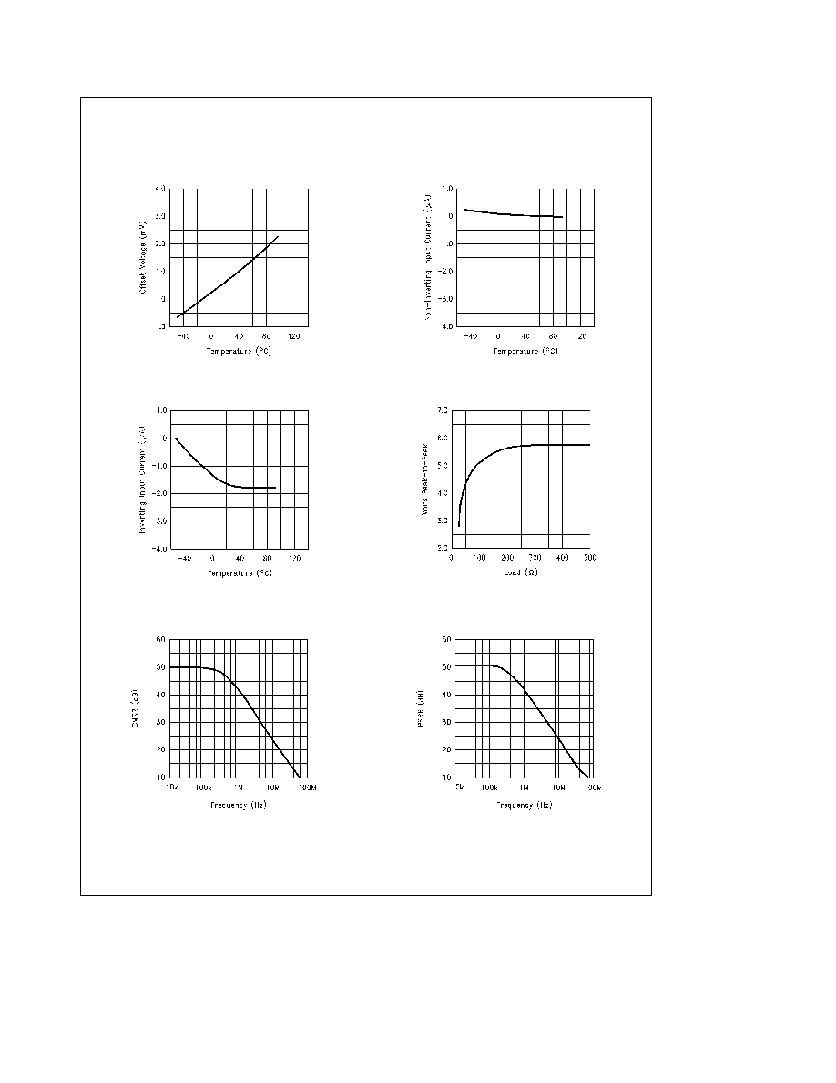
Typical Performance Characteristics
A
V
e a
2 R
F
e
348X V
a e a
5V V
b e b
5V R
L
e
100X T
J
e
25 C unless otherwise noted
Voltage vs Temperature
LM6310 Input Offset
TL H 12545 3
Current vs Temperature
LM6310 Non-Inverting Input
TL H 12545 4
Current vs Temperature
LM6310 Inverting Input
TL H 12545 5
vs Load (Volts Peak-to-Peak)
Output Voltage Swing
TL H 12545 6
LM6310 Common Mode
Rejection Ratio vs Frequency
TL H 12545 7
LM6310 Power Supply
Rejection Ratio vs Frequency
TL H 12545 8
http
www national com
4
Typical Performance Characteristics
A
V
e a
2 R
F
e
348X V
a e a
5V V
b e b
5V R
L
e
100X T
J
e
25 C unless otherwise noted (Continued)
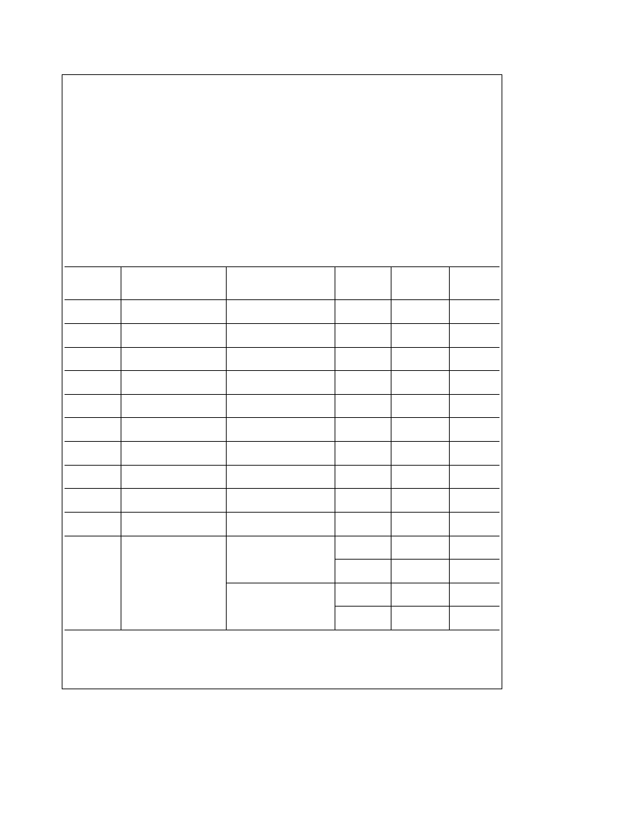
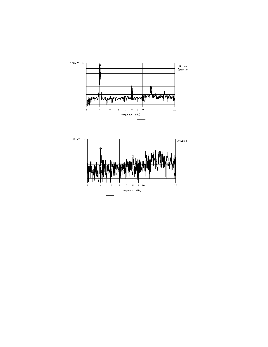
Output Signal Isolation in Disable Mode
Reference
Level
e
100 mV
Marker
4 025 567 Hz
68 8755 mV
TL H 12545 9
LM6310 Normal Operation Disable
e
High
Note reference level is 100 mV
4 MHz signal is at 69 mV
Reference
Level
e
50 mV
Marker
4 025 567 Hz
28 9085 mV
TL H 12545 10
LM6310 Disable
e
Low
Note that the reference level is 50 mV
The 4 MHz signal is near the noise level attenuated
l
1000 1
http
www national com
5