TL H 11979
LM6104
Quad
Gray
Scale
Current
Feedback
Amplifier
June 1994
LM6104
Quad Gray Scale Current Feedback Amplifier
General Description
The LM6104 quad amplifier meets the requirements of bat-
tery operated liquid crystal displays by providing high speed
while maintaining low power consumption
Combining this high speed with high integration
the
LM6104 conserves valuable board space in portable sys-
tems with a cost effective surface mount quad package
Built on National's advanced high speed VIP
TM
(Vertically
Integrated PNP) process the LM6104 current feedback ar-
chitecture is easily compensated for speed and loading con-
ditions These features make the LM6104 ideal for buffering
grey levels in liquid crystal displays
Features
(Typical unless otherwise noted)
Y
Low power
I
S
e
875 mA amplifier
Y
Slew rate
100V ms
Y
b
3dB bandwidth (R
F
e
1 kX)
30 MHz
Y
High output drive
g
5V into 100X
Y
Wide operating range
V
S
e
5V to
g
12V
Y
High integration
Quad surface mount
Applications
Y
Grey level buffer for liquid crystal displays
Y
Column buffer for portable LCDs
Y
Video distribution amplifiers video line drivers
Y
Hand-held high speed signal conditioning
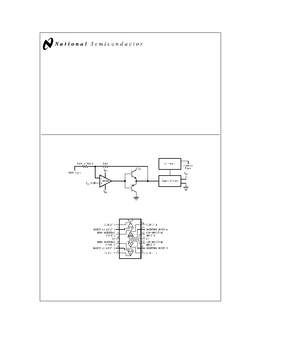
Typical Application
LCD Buffer Application for Grey Levels
TL H 11979 Ł 1
Connection Diagram
TL H 11979 Ł 2
Order Number LM6104M
See NS Package Number M14A
VIP
TM
is a trademark of National Semiconductor Corporation
C1995 National Semiconductor Corporation
RRD-B30M115 Printed in U S A
Absolute Maximum Ratings
(Note 1)
If Military Aerospace specified devices are required
please contact the National Semiconductor Sales
Office Distributors for availability and specifications
Supply Voltage
24V
Differential Input Voltage
g
6V
Input Voltage
g
Supply Voltage
Inverting Input Current
15 mA
Soldering Information
Vapor Phase (60s)
215 C
Infrared (15s)
220 C
Storage Temperature Range
b
65 C
s
T
J
s
a
150 C
Maximum Junction Temperature
150 C
ESD Rating (Note 2)
2000V
Operating Ratings
Supply Voltage Range
4 75V to 24V
Junction Temperature Range (Note 3)
LM6104M
b
20
s
T
J
s
a
80 C
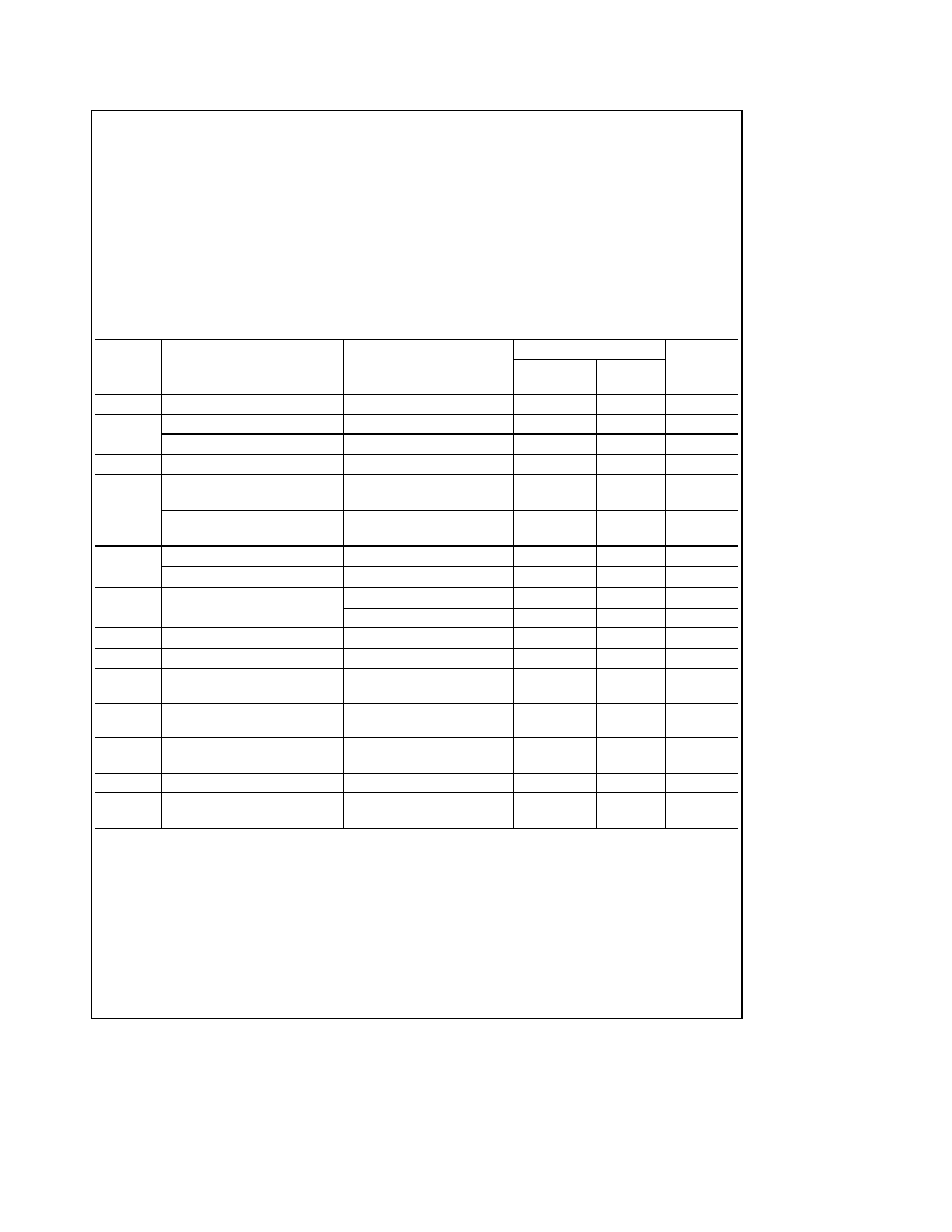
Electrical Characteristics
The following specifications apply for V
a e
8V V
b e b
5V R
L
e
R
F
e
2 kX and 0
s
T
J
s
60 C unless otherwise noted
Symbol
Parameter
Conditions
LM6104M
Units
Typical
Limits
(Note 4)
(Note 5)
V
OS
Input Offset Voltage
10
30
mV max
I
B
Inverting Input Bias Current
5 0
20
m
A max
Non-Inverting Input Bias Current
0 5
2
m
A max
I
S
Supply Current
V
O
e
0V
3 5
4 0
mA max
I
SC
Output Source Current
V
O
e
0V
60
45
mA
I
IN(b)
e b
100 mA
min
Output Sink Current
V
O
e
0V
60
45
mA
I
IN(b)
e
100 mA
min
V
O
Positive Output Swing
I
IN(b)
e b
100 mA
6 5
6 1
V min
Negative Output Swing
I
IN(b)
e
100 mA
b
3 5
b
3 1
V max
PSRR
Power Supply Rejection Ratio
V
S
e
g
4 to
g
10V
70
60
dB min
100 mV pp
100 kHz
40
30
dB min
R
T
Transresistance
10
5
MX min
SR
Slew Rate
(Note 6)
100
55
V ms min
BW
Bandwidth
A
V
e b
1
7 5
5 0
MHz
R
IN
e
R
F
e
2 kX
Amp-to-Amp Isolation
R
L
e
2 kX
60
dB
F
e
1 MHz
CMVR
Common Mode Voltage Range
V
a
b
1 4V
V
V
b
a
1 4V
CMRR
Common Mode Rejection Ratio
60
dB
t
S
Settling Time
0 05% 5V Step A
V
e b
1
240
ns
R
F
e
R
S
e
2 kX V
S
e
g
5V
Note 1
Absolute Maximum Ratings indicate limits beyond which damage to the device may occur DC and AC electrical specifications do not apply when operating
the device beyond its rated operating conditions Operating ratings indicate conditions the device is intended to be functional but device parameter specifications
may not be guaranteed under the conditions
Note 2
Human body model 1 5 kX and 100 pF This is a class 2 device rating
Note 3
Thermal resistance of the SO package is 98 C W When operating at T
A
e
80 C maximum power dissipation is 700 mW
Note 4
Typical values represent the most likely parametric norm
Note 5
All limits guaranteed at operating temperature extremes
Note 6
A
V
e b
1 with R
IN
e
R
F
e
2 kX Slew rate is calculated from the 25% to the 75% point on both rising and falling edges Output swing is
b
0 6V to
a
5 6V
and 5 6V to 0 6V
2

Typical Performance Characteristics
Closed Loop Gain
Frequency Response vs
Amplifier Isolation
Amplifier to
Supply Voltage
Supply Current vs
A
V
e b
1
Large Signal Pulse Response
A
V
e b
1 R
F
e
R
G
Frequency Response vs R
F
I
IN
e
g
100 mA
V
S
e
g
5V
V
OUT
Referred to Supplies
vs Source Current
LM6104 Output Voltage
vs Sink Current
LM6104 Output Voltage
TL H 11979 Ł 3
3

Applications Information
CURRENT FEEDBACK TOPOLOGY
The small-signal bandwidth of conventional voltage feed-
back amplifiers is inversely proportional to the closed-loop
gain based on the gain-bandwidth concept In contrast the
current feedback amplifier topology such as the LM6104
enables a signal bandwidth that is relatively independent of
the amplifier's gain (see typical curve Frequency Response
vs Closed Loop Gain)
FEEDBACK RESISTOR SELECTION R
F
Current feedback amplifier bandwidth and slew rate are
controlled by R
F
R
F
and the amplifier's internal compensa-
tion capacitor set the dominant pole in the frequency re-
sponse The amplifier therefore always requires a feed-
back resistor even in unity gain
Bandwidth and slew rate are inversely proportional to the
value of R
F
(see typical curve Frequency Response vs R
F
)
This makes the amplifier especially easy to compensate for
a desired pulse response (see typical curve Large Signal
Pulse Response) Increased capacitive load driving capabili-
ty is also achieved by increasing the value of R
F
The LM6104 has guaranteed performance with a feedback
resistor of 2 kX
CAPACITIVE FEEDBACK
It is common to place a small lead capacitor in parallel with
feedback resistance to compensate voltage feedback am-
plifiers Do not place a capacitor across R
F
to limit the band-
width of current feedback amplifiers The dynamic imped-
ance of capacitors in the feedback path of the LM6104 as
with any current feedback amplifier will cause instability
4

5