TL H 7854
LM566C
Voltage
Controlled
Oscillator
February 1995
LM566C Voltage Controlled Oscillator
General Description
The LM566CN is a general purpose voltage controlled oscil-
lator which may be used to generate square and triangular
waves the frequency of which is a very linear function of a
control voltage The frequency is also a function of an exter-
nal resistor and capacitor
The LM566CN is specified for operation over the 0 C to
a
70 C temperature range
Features
Y
Wide supply voltage range 10V to 24V
Y
Very linear modulation characteristics
Y
High temperature stability
Y
Excellent supply voltage rejection
Y
10 to 1 frequency range with fixed capacitor
Y
Frequency programmable by means of current voltage
resistor or capacitor
Applications
Y
FM modulation
Y
Signal generation
Y
Function generation
Y
Frequency shift keying
Y
Tone generation
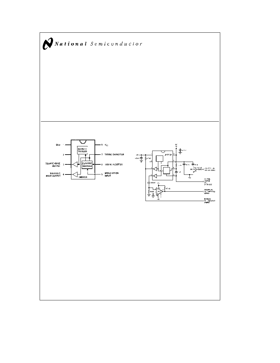
Connection Diagram
Dual-In-Line Package
TL H 7854 Ł 2
Order Number LM566CN
See NS Package Number N08E
Typical Application
1 kHz and 10 kHz TTL Compatible
Voltage Controlled Oscillator
TL H 7854 Ł 3
C1995 National Semiconductor Corporation
RRD-B30M115 Printed in U S A
Absolute Maximum Ratings
If Military Aerospace specified devices are required
please contact the National Semiconductor Sales
Office Distributors for availability and specifications
Power Supply Voltage
26V
Power Dissipation (Note 1)
1000 mW
Operating Temperature Range LM566CN
0 C to
a
70 C
Lead Temperature (Soldering 10 sec )
a
260 C
Electrical Characteristics
V
CC
e
12V T
A
e
25 C AC Test Circuit
Parameter
Conditions
LM566C
Units
Min
Typ
Max
Maximum Operating
R0
e
2k
0 5
1
MHz
Frequency
C0
e
2 7 pF
VCO Free-Running
C
O
e
1 5 nF
Frequency
R
O
e
20k
b
30
0
a
30
%
f
O
e
10 kHz
Input Voltage Range Pin 5
V
CC
V
CC
Average Temperature Coefficient
200
ppm C
of Operating Frequency
Supply Voltage Rejection
10 Ł 20V
0 1
2
% V
Input Impedance Pin 5
0 5
1
MX
VCO Sensitivity
For Pin 5 From
6 0
6 6
7 2
kHz V
8 Ł 10V f
O
e
10 kHz
FM Distortion
g
10% Deviation
0 2
1 5
%
Maximum Sweep Rate
1
MHz
Sweep Range
10 1
Output Impedance
Pin 3
50
X
Pin 4
50
X
Square Wave Output Level
R
L1
e
10k
5 0
5 4
Vp-p
Triangle Wave Output Level
R
L2
e
10k
2 0
2 4
Vp-p
Square Wave Duty Cycle
40
50
60
%
Square Wave Rise Time
20
ns
Square Wave Fall Time
50
ns
Triangle Wave Linearity
a
1V Segment at
0 5
%
V
CC
Note 1
The maximum junction temperature of the LM566CN is 150 C For operation at elevated junction temperatures maximum power dissipation must be
derated based on a thermal resistance of 115 C W junction to ambient
Applications Information
The LM566CN may be operated from either a single supply
as shown in this test circuit or from a split (
g
) power sup-
ply When operating from a split supply the square wave
output (pin 3) is TTL compatible (2 mA current sink) with the
addition of a 4 7 kX resistor from pin 3 to ground
A 0 001 mF capacitor is connected between pins 5 and 6 to
prevent parasitic oscillations that may occur during VCO
switching
f
O
e
2 4(V
a
b
V
5
)
R
O
C
O
V
a
where
2K
k
R
O
k
20K
and V
5
is voltage between pin 5 and pin 1
2
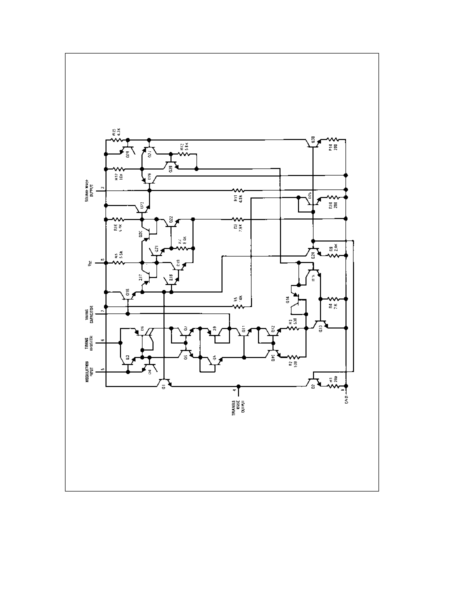
Schematic Diagram
TLH7854
Ł
1
3
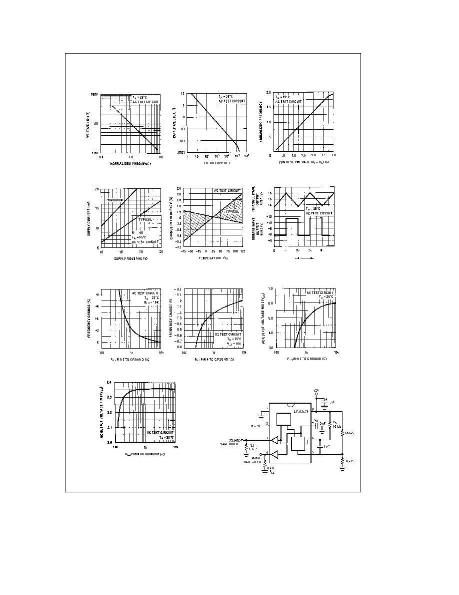
Typical Performance Characteristics
Function of Timing Resistor
Operating Frequency as a
Function of Timing Capacitor
Operating Frequency as a
Function of Control Voltage
Normalized Frequency as a
Power Supply Current
Temperature Stability
VCO Waveforms
Output)
Resistance (Square Wave
Frequency Stability vs Load
Impedance (Triangle Output)
Frequency Stability vs Load
Characteristics
Square Wave Output
TL H 7854 Ł 4
Characteristics
Triangle Wave Output
TL H 7854 Ł 5
AC Test Circuit
TL H 7854 Ł 6
4

5