LM565/LM565C
Phase Locked Loop
General Description
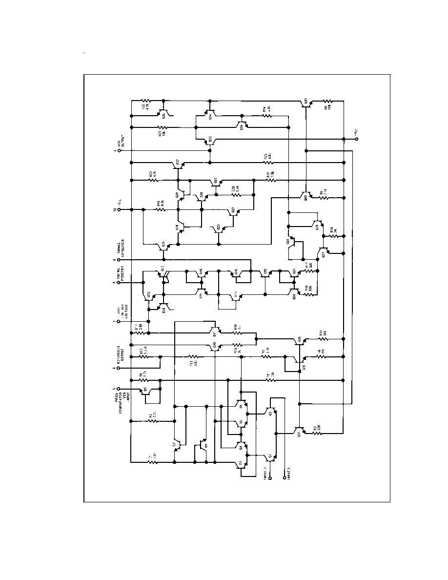
The LM565 and LM565C are general purpose phase locked
loops containing a stable, highly linear voltage controlled os-
cillator for low distortion FM demodulation, and a double bal-
anced phase detector with good carrier suppression. The
VCO frequency is set with an external resistor and capacitor,
and a tuning range of 10:1 can be obtained with the same
capacitor.
The
characteristics
of
the
closed
loop
system -- bandwidth, response speed, capture and pull in
range -- may be adjusted over a wide range with an external
resistor and capacitor. The loop may be broken between the
VCO and the phase detector for insertion of a digital fre-
quency divider to obtain frequency multiplication.
The LM565H is specified for operation over the -55¯C to
+125¯C military temperature range. The LM565CN is speci-
fied for operation over the 0¯C to +70¯C temperature range.
Features
n
200 ppm/¯C frequency stability of the VCO
n
Power supply range of
Ý
5 to
Ý
12 volts with 100 ppm/%
typical
n
0.2% linearity of demodulated output
n
Linear triangle wave with in phase zero crossings
available
n
TTL and DTL compatible phase detector input and
square wave output
n
Adjustable hold in range from
Ý
1% to
>
Ý
60%
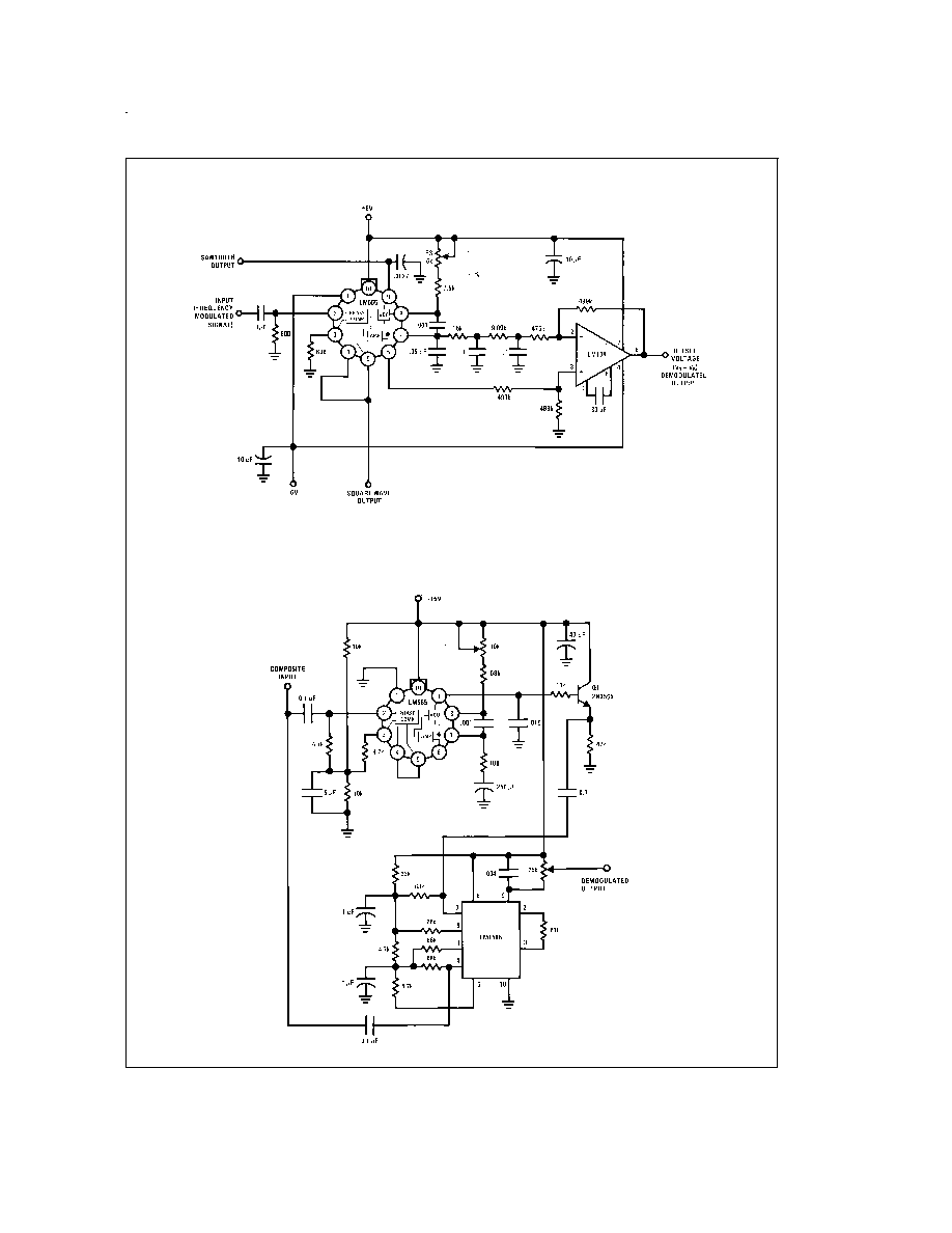
Applications
n
Data and tape synchronization
n
Modems
n
FSK demodulation
n
FM demodulation
n
Frequency synthesizer
n
Tone decoding
n
Frequency multiplication and division
n
SCA demodulators
n
Telemetry receivers
n
Signal regeneration
n
Coherent demodulators
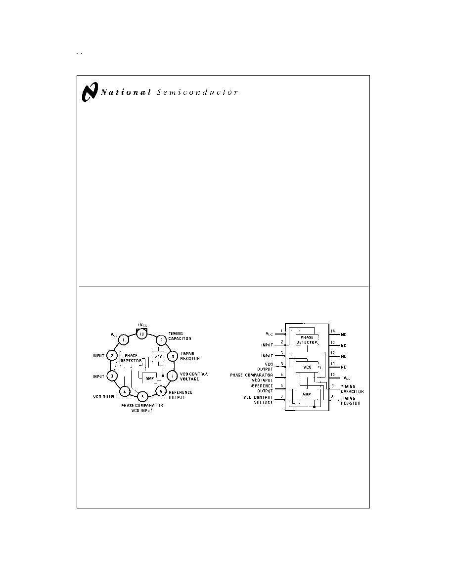
Connection Diagrams
Metal Can Package
DS007853-2
Order Number LM565H
See NS Package Number H10C
Dual-in-Line Package
DS007853-3
Order Number LM565CN
See NS Package Number N14A
May 1999
LM565/LM565C
Phase
Locked
Loop
ˋ 1999 National Semiconductor Corporation
DS007853
www.national.com

Absolute Maximum Ratings
(Note 1)
If Military/Aerospace specified devices are required,
please contact the National Semiconductor Sales Office/
Distributors for availability and specifications.
Supply Voltage
Ý
12V
Power Dissipation (Note 2)
1400 mW
Differential Input Voltage
Ý
1V
Operating Temperature Range
LM565H
-55¯C to +125¯C
LM565CN
0¯C to +70¯C
Storage Temperature Range
-65¯C to +150¯C
Lead Temperature
(Soldering, 10 sec.)
260¯C
Electrical Characteristics
AC Test Circuit, T
A
= 25¯C, V
CC
=
Ý
6V
Parameter
Conditions
LM565
LM565C
Units
Min
Typ
Max
Min
Typ
Max
Power Supply Current
8.0
12.5
8.0
12.5
mA
Input Impedance (Pins 2, 3)
-4V
<
V
2
, V
3
<
0V
7
10
5
k
VCO Maximum Operating
Frequency
C
o
= 2.7 pF
300
500
250
500
kHz
VCO Free-Running Frequency
C
o
= 1.5 nF
R
o
= 20 k
f
o
= 10 kHz
-10
0
+10
-30
0
+30
%
Operating Frequency
Temperature Coefficient
-100
-200
ppm/¯C
Frequency Drift with
Supply Voltage
0.1
1.0
0.2
1.5
%/V
Triangle Wave Output Voltage
2
2.4
3
2
2.4
3
V
p-p
Triangle Wave Output Linearity
0.2
0.5
%
Square Wave Output Level
4.7
5.4
4.7
5.4
V
p-p
Output Impedance (Pin 4)
5
5
k
Square Wave Duty Cycle
45
50
55
40
50
60
%
Square Wave Rise Time
20
20
ns
Square Wave Fall Time
50
50
ns
Output Current Sink (Pin 4)
0.6
1
0.6
1
mA
VCO Sensitivity
f
o
= 10 kHz
6600
6600
Hz/V
Demodulated Output Voltage
(Pin 7)
Ý
10% Frequency Deviation
250
300
400
200
300
450
mV
p-p
Total Harmonic Distortion
Ý
10% Frequency Deviation
0.2
0.75
0.2
1.5
%
Output Impedance (Pin 7)
3.5
3.5
k
DC Level (Pin 7)
4.25
4.5
4.75
4.0
4.5
5.0
V
Output Offset Voltage
|V
7
- V
6
|
30
100
50
200
mV
Temperature Drift of |V
7
- V
6
|
500
500
çV/¯C
AM Rejection
30
40
40
dB
Phase Detector Sensitivity K
D
0.68
0.68
V/radian
Note 1: Absolute Maximum Ratings indicate limits beyond which damage to the device may occur. Operating Ratings indicate conditions for which the device is func-
tional, but do not guarantee specific performance limits. Electrical Characteristics state DC and AC electrical specifications under particular test conditions which guar-
antee specific performance limits. This assumes that the device is within the Operating Ratings. Specifications are not guaranteed for parameters where no limit is
given, however, the typical value is a good indication of device performance.
Note 2: The maximum junction temperature of the LM565 and LM565C is +150¯C. For operation at elevated temperatures, devices in the TO-5 package must be
derated based on a thermal resistance of +150¯C/W junction to ambient or +45¯C/W junction to case. Thermal resistance of the dual-in-line package is +85¯C/W.
www.national.com
2

Typical Performance Characteristics
Power Supply Current as a
Function of Supply Voltage
DS007853-14
Lock Range as a Function
of Input Voltage
DS007853-15
VCO Frequency
DS007853-16
Oscillator Output
Waveforms
DS007853-17
Phase Shift vs Frequency
DS007853-18
VCO Frequency as a
Function of Temperature
DS007853-19
Loop Gain vs Load
Resistance
DS007853-20
Hold in Range as a
Function of R
6Ù7
DS007853-21
www.national.com
3