LM5642
High Voltage, Dual Synchronous Buck Converter with
Oscillator Synchronization
General Description
The LM5642 consists of two current mode synchronous
buck regulator controllers operating 180° out of phase with
each other at a normal switching frequency of 200kHz.
Out of phase operation reduces the input ripple RMS cur-
rent, thereby significantly reducing the required input capaci-
tance. The switching frequency can be synchronized to an
external clock between 150kHz and 250kHz. The two switch-
ing regulator outputs can also be paralleled to operate as a
dual-phase single output regulator.
The output of each channel can be independently adjusted
from 1.3 to 90% of Vin. An internal 5V rail is also available
externally for driving bootstrap circuitry.
Current-mode feedback control assures excellent line and
load regulation and a wide loop bandwidth for excellent
response to fast load transients. Current is sensed across
either the Vds of the top FET or across an external current-
sense resistor connected in series with the drain of the top
FET.
The LM5642 features analog soft-start circuitry that is inde-
pendent of the output load and output capacitance making
the soft-start behavior more predictable and controllable
than traditional soft-start circuits.
Over-voltage protection is available for both outputs. A UV-
Delay pin is also available to allow delayed shut off time for
the IC during an output under-voltage event.
Features
n
Two synchronous buck regulators
n
180° out of phase operation
n
Synchronizable switching frequency from 150kHz to
250kHz
n
4.5V to 36V input range
n
50µA Shutdown current
n
Adjustable output from 1.3V to 90% of Vin
n
0.04% (typical) line and load regulation error
n
Current mode control with or without a sense resistor
n
Independent enable/soft-start pins allow simple
sequential startup configuration.
n
Configurable for single output parallel operation. (See
Figure 2)
n
Adjustable cycle-by-cycle current limit
n
Input under-voltage lockout
n
Output over-voltage latch protection
n
Output under-voltage protection with delay
n
Thermal shutdown
n
Self discharge of output capacitors when the regulator is
OFF
n
TSSOP package
Applications
n
Embedded Computer Systems
n
Telecom Systems
n
Set-Top Boxes
n
WebPAD
n
Point Of Load Power Architectures
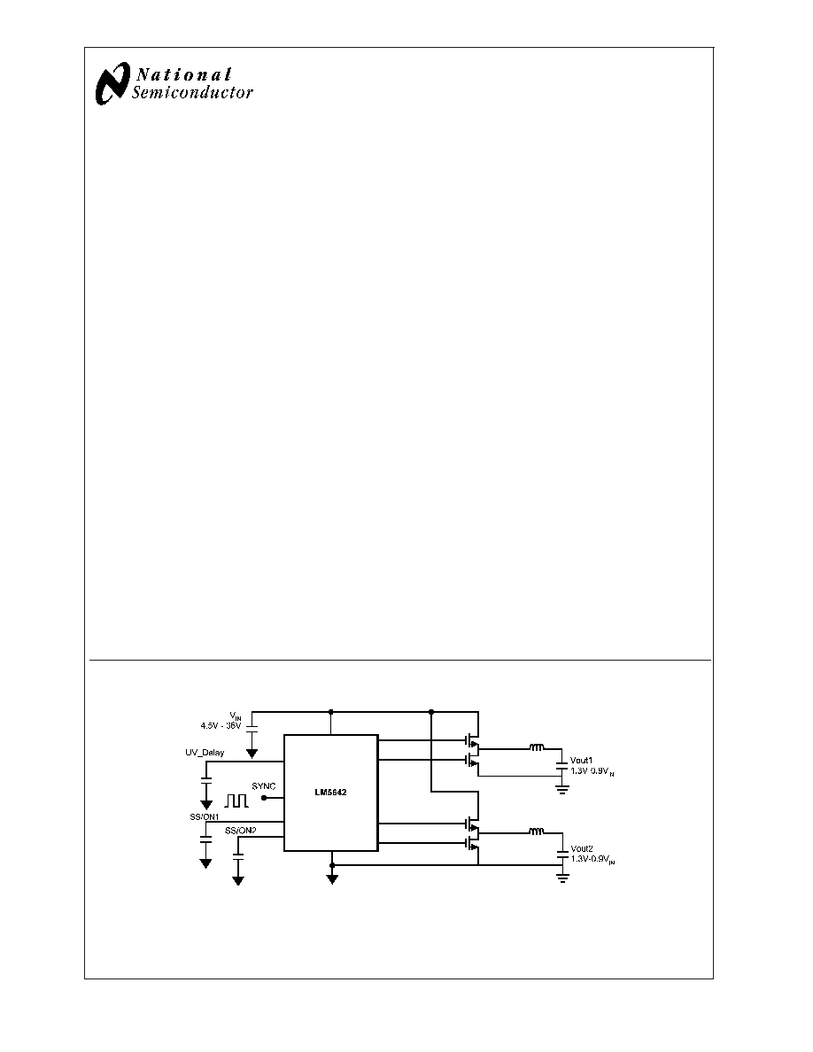
Typical Application Circuit
20060101
September 2003
LM5642
High
V
oltage,
Dual
Synchronous
Buck
Converter
with
Oscillator
Synchronization
© 2003 National Semiconductor Corporation
DS200601
www.national.com
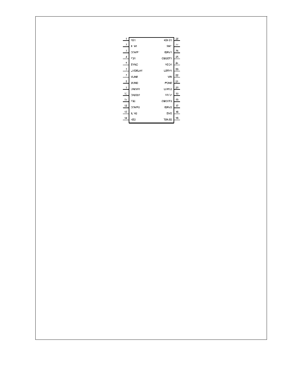
Connection Diagram
TOP VIEW
20060102
28-Lead TSSOP (MTC)
Order Number LM5642MTC
See NS Package Number MTC28
Pin Descriptions
KS1 (Pin 1): The positive (+) Kelvin sense for the internal
current sense amplifier of Channel 1. Use a separate trace to
connect this pin to the current sense point. It should be
connected to VIN as close as possible to the node of the
current sense resistor. When no current-sense resistor is
used, connect as close as possible to the drain node of the
upper MOSFET.
ILIM1 (Pin 2): Current limit threshold setting for Channel 1. It
sinks a constant current of 9.9µA, which is converted to a
voltage across a resistor connected from this pin to VIN. The
voltage across the resistor is compared with either the V
DS
of the top MOSFET or the voltage across the external cur-
rent sense resistor to determine if an over-current condition
has occurred in Channel 1.
COMP1 (Pin 3): Compensation pin for Channel 1. This is the
output of the internal transconductance amplifier. The com-
pensation network should be connected between this pin
and the signal ground, SGND (Pin 8).
FB1 (Pin 4): Feedback input for channel 1. Connect to
VOUT through a voltage divider to set the Channel 1 output
voltage.
SYNC (Pin 5): The switching frequency of the LM5642 can
be synchronized to an external clock.
SYNC = LOW: Free running at 200kHz, channels are 180°
out of phase.
SYNC = HIGH: Waiting for external clock
SYNC = Falling Edge: Channel 1 HDRV pin goes high.
Channel 2 HDRV pin goes high after 2.5µs delay. The maxi-
mum SYNC pulse width must be greater than 100ns.
For SYNC = Low operation, connect this pin to signal ground
through a 220k
resistor.
UV_DELAY (Pin 6): A capacitor from this pin to ground sets
the delay time for UVP. The capacitor is charged from a 5µA
current source. When UV_DELAY charges to 2.3V (typical),
the system immediately latches off. Connecting this pin to
ground will disable the output under-voltage protection.
VLIN5 (Pin 7): The output of an internal 5V LDO regulator
derived from VIN. It supplies the internal bias for the chip and
supplies the bootstrap circuitry for gate drive. Bypass this pin
to signal ground with a minimum of 4.7µF ceramic capacitor.
SGND (Pin 8): The ground connection for the signal-level
circuitry. It should be connected to the ground rail of the
system.
ON/SS1 (Pin 9): Channel 1 enable pin. This pin is internally
pulled up to one diode drop above VLIN5. Pulling this pin
below 1.2V (open-collector type) turns off Channel 1. If both
ON/SS1 and ON/SS2 pins are pulled below 1.2V, the whole
chip goes into shut down mode. Adding a capacitor to this
pin provides a soft-start feature that minimizes inrush current
and output voltage overshoot.
ON/SS2 (Pin 10): Channel 2 enable pin. See the description
for Pin 9, ON/SS1. May be connected to ON/SS1 for simul-
taneous startup or for parallel operation.
FB2 (Pin 11): Feedback input for channel 2. Connect to
VOUT through a voltage divider to set the Channel 2 output
voltage.
COMP2 (Pin 12): Compensation pin for Channel 2. This is
the output of the internal transconductance amplifier. The
compensation network should be connected between this
pin and the signal ground SGND (Pin 8).
ILIM2 (Pin 13): Current limit threshold setting for Channel 2.
See ILIM1 (Pin 2).
KS2 (Pin 14): The positive (+) Kelvin sense for the internal
current sense amplifier of Channel 2. See KS1 (Pin 1).
RSNS2 (Pin 15): The negative (-) Kelvin sense for the
internal current sense amplifier of Channel 2. Connect this
pin to the low side of the current sense resistor that is placed
between VIN and the drain of the top MOSFET. When the
LM5642
www.national.com
2

Pin Descriptions
(Continued)
Rds of the top MOSFET is used for current sensing, connect
this pin to the source of the top MOSFET. Always use a
separate trace to form a Kelvin connection to this pin.
SW2 (Pin 16): Switch-node connection for Channel 2, which
is connected to the source of the top MOSFET of Channel 2.
It serves as the negative supply rail for the top-side gate
driver, HDRV2.
HDRV2 (Pin 17): Top-side gate-drive output for Channel 2.
HDRV is a floating drive output that rides on the correspond-
ing switching-node voltage.
CBOOT2 (Pin 18): Bootstrap capacitor connection. It serves
as the positive supply rail for the Channel 2 top-side gate
drive. Connect this pin to VDD2 (Pin 19) through a diode,
and connect the low side of the bootstrap capacitor to SW2
(Pin16).
VDD2 (Pin 19): The supply rail for the Channel 2 low-side
gate drive. Connected to VLIN5 (Pin 7) through a 4.7
resistor and bypassed to power ground with a ceramic ca-
pacitor of at least 1µF. Tie this pin to VDD1 (Pin 24).
LDRV2 (Pin 20): Low-side gate-drive output for Channel 2.
PGND (Pin 21): The power ground connection for both
channels. Connect to the ground rail of the system.
VIN (Pin 22): The power input pin for the chip. Connect to
the positive (+) input rail of the system. This pin must be
connected to the same voltage rail as the top FET drain (or
the current sense resistor when used).
LDRV1 (Pin 23): Low-side gate-drive output for Channel 1.
VDD1 (Pin 24): The supply rail for Channel 1 low-side gate
drive. Tie this pin to VDD2 (Pin 19).
CBOOT1 (Pin 25): : Bootstrap capacitor connection. It
serves as the positive supply rail for Channel 1 top-side gate
drive. See CBOOT2 (Pin 18).
HDRV1 (Pin 26): Top-side gate-drive output for Channel 1.
See HDRV2 (Pin 17).
SW1 (Pin 27): Switch-node connection for Channel 1. See
SW2 (Pin16).
RSNS1 (Pin 28): The negative (-) Kelvin sense for the
internal current sense amplifier of Channel 1. See RSNS2
(Pin 15).
LM5642
www.national.com
3
Absolute Maximum Ratings
(Note 1)
If Military/Aerospace specified devices are required,
please contact the National Semiconductor Sales Office/
Distributors for availability and specifications.
Voltages from the indicated pins to SGND/PGND:
VIN, ILIM1, ILIM2, KS1, KS2
-0.3V to 38V
SW1, SW2, RSNS1, RSNS2
-0.3 to (V
IN
+
0.3)V
FB1, FB2, VDD1, VDD2
-0.3V to 6V
SYNC, COMP1, COMP2, UV Delay
-0.3V to (VLIN5
+0.3)V
ON/SS1, ON/SS2 (Note 2)
-0.3V to (VLIN5
+0.6)V
CBOOT1, CBOOT2
43V
CBOOT1 to SW1, CBOOT2 to SW2
-0.3V to 7V
LDRV1, LDRV2
-0.3V to
(VDD+0.3)V
HDRV1 to SW1, HDRV2 to SW2
-0.3V
HDRV1 to CBOOT1, HDRV2 to
CBOOT2
+0.3V
Power Dissipation (T
A
= 25°C),
(Note 3)
1.1W
Ambient Storage Temperature
Range
-65°C to +150°C
Soldering Dwell Time, Temperature
(Note 4)
Wave
Infrared
Vapor Phase
4 sec, 260°C
10sec, 240°C
75sec, 219°C
ESD Rating (Note 5)
2kV
Operating Ratings
(Note 1)
VIN (VLIN5 tied to VIN)
4.5V to 5.5V
VIN (VIN and VLIN5 separate)
5.5V to 36V
Junction Temperature
-40°C to +125°C
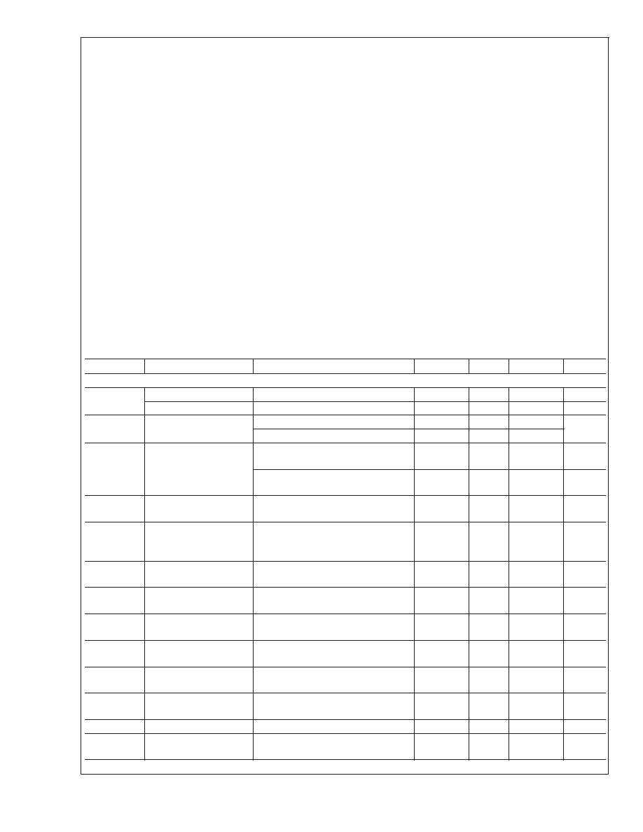
Electrical Characteristics
Unless otherwise specified, V
IN
= 28V, GND = PGND = 0V, VLIN5 = VDD1 = VDD2. Limits appearing in boldface type apply
over the specified operating junction temperature range, (-40°C to +125°C, if not otherwise specified). Specifications appearing
in plain type are measured using low duty cycle pulse testing with T
A
= 25°C (Note 6), (Note 7). Min/Max limits are guaranteed
by design, test, or statistical analysis.
Symbol
Parameter
Conditions
Min
Typ
Max
Units
System
V
OUT
/V
OUT
Load Regulation
VIN = 28V, V
compx
= 0.5V to 1.5V
0.04
%
Line Regulation
5.5V
VIN 36V, V
compx
=1.25V
0.04
%
V
FB1_FB2
Feedback Voltage
5.5V
VIN 36V
1.2154
1.2364
1.2574
V
-20°C to 85°C
1.2179
1.2364
1.2549
I
VIN
Input Supply Current
V
ON_SSx
>
2V
5.5V
VIN 36V
1.1
2.0
mA
Shutdown (Note 8)
V
ON_SS1
= V
ON_SS2
= 0V
50
110
µA
VLIN5
VLIN5 Output Voltage
IVLIN5 = 0 to 25mA,
5.5V
VIN 36V
4.70
5
5.30
V
V
CLos
Current Limit
Comparator Offset
(VILIMX -VRSNSX)
V
IN
= 6V
±
2
±
7.0
mV
I
CL
Current Limit Sink
Current
8.4
9.9
11.4
µA
I
ss_SC1
,
I
ss_SC2
Soft-Start Source
Current
V
ON_ss1
= V
ON_ss2
= 1.5V (on)
0.5
2.4
5.0
µA
I
ss_SK1
,
I
ss_SK2
Soft-Start Sink Current
V
ON_ss1
= V
ON_ss2
= 1.5V
2
5.5
10
µA
V
ON_SS1
,
V
ON_SS2
Soft-Start On Threshold
0.7
1.12
1.4
V
V
SSTO
Soft-Start Timeout
Threshold
(Note 9)
3.4
V
I
sc_uvdelay
UV_DELAY Source
Current
UV-DELAY = 2V
2
5
9
µA
I
sk_uvdelay
UV_DELAY Sink Current
UV-DELAY = 0.4V
0.2
0.48
1.2
mA
V
UVDelay
UV_DELAY Threshold
Voltage
2.3
V
LM5642
www.national.com
4
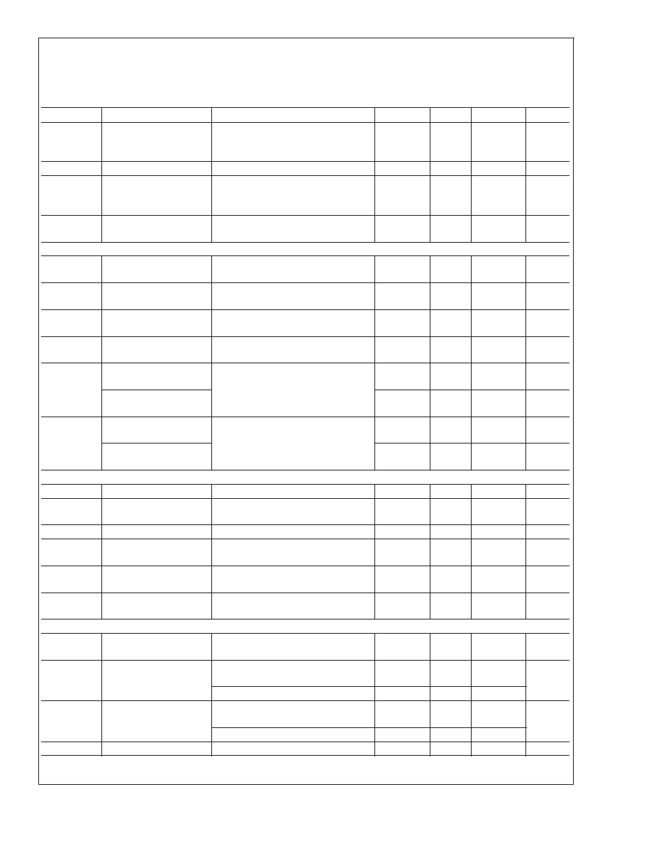
Electrical Characteristics
(Continued)
Unless otherwise specified, V
IN
= 28V, GND = PGND = 0V, VLIN5 = VDD1 = VDD2. Limits appearing in boldface type apply
over the specified operating junction temperature range, (-40°C to +125°C, if not otherwise specified). Specifications appearing
in plain type are measured using low duty cycle pulse testing with T
A
= 25°C (Note 6), (Note 7). Min/Max limits are guaranteed
by design, test, or statistical analysis.
Symbol
Parameter
Conditions
Min
Typ
Max
Units
V
UVP
FB1, FB2, Under
Voltage Protection Latch
Threshold
As a percentage of nominal output
voltage (falling edge)
75
80.7
86
%
Hysteresis
3.7
%
V
OVP
V
OUT
Overvoltage
Shutdown Latch
Threshold
As a percentage measured at V
FB1
,
V
FB2
107
114
122
%
S
wx_R
SW1, SW2
ON-Resistance
V
SW1
= V
SW2
= 0.4V
420
487
560
Gate Drive
I
CBOOT
CBOOTx Leakage
Current
V
CBOOT1
= V
CBOOT2
= 7V
10
nA
I
SC_DRV
HDRVx and LDRVx
Source Current
V
CBOOT1
= V
CBOOT2
= 5V, VSWx=0V,
HDRVx=LDRVx=2.5V
0.5
A
I
sk_HDRV
HDRVx Sink Current
V
CBOOTx
= VDDx = 5V, V
SWx
= 0V,
HDRVX = 2.5V
0.8
A
I
sk_LDRV
LDRVx Sink Current
V
CBOOTx
= VDDx = 5V, V
SWx
= 0V,
LDRVX = 2.5V
1.1
A
R
HDRV
HDRV1 & 2 Source
On-Resistance
V
CBOOT1
= V
CBOOT2
= 5V,
V
SW1
= V
SW2
= 0V
3.1
HDRV1 & 2 Sink
On-Resistance
1.5
R
LDRV
LDRV1 & 2 Source
On-Resistance
V
CBOOT1
= V
CBOOT2
= 5V,
V
SW1
= V
SW2
= 0V
V
DD1
= V
DD1
= 5V
3.1
LDRV1 & 2 Sink
On-Resistance
1.1
Oscillator and Sync Controls
F
osc
Oscillator Frequency
5.5
V
IN
36V
166
200
226
kHz
Don_max
Maximum On-Duty Cycle
V
FB1
= V
FB2
= 1V, Measured at pins
HDRV1 and HDRV2
96
98.9
%
T
on_min
Minimum On-Time
166
ns
SS
OT_delta
HDRV1 and HDRV2
Delta On Time
ON/SS1 = ON/SS2 = 2V
20
250
ns
V
HS
SYNC Pin Min High
Input
2
1.52
V
V
LS
SYNC Pin Max Low
Input
1.44
0.8
V
Error Amplifier
I
FB1
, I
FB2
Feedback Input Bias
Current
V
FB1_FIX
= 1.5V, V
FB2_FIX
= 1.5V
80
±
200
nA
I
comp1_SC
,
I
comp2_SC
COMP Output Source
Current
V
FB1_FIX
= V
FB2_FIX
= 1V,
V
COMP1
= V
COMP2
= 1V
6
127
µA
-20°C to 85°C
18
I
comp1_SK
,
I
comp2_SK
COMP Output Sink
Current
V
FB1_FIX
= V
FB2_FIX
= 1.5V and
V
COMP1
= V
COMP2
= 0.5V
6
118
µA
-20°C to 85°C
18
gm1, gm2
Transconductance
720
µmho
LM5642
www.national.com
5