LM56
Dual Output Low Power Thermostat
General Description
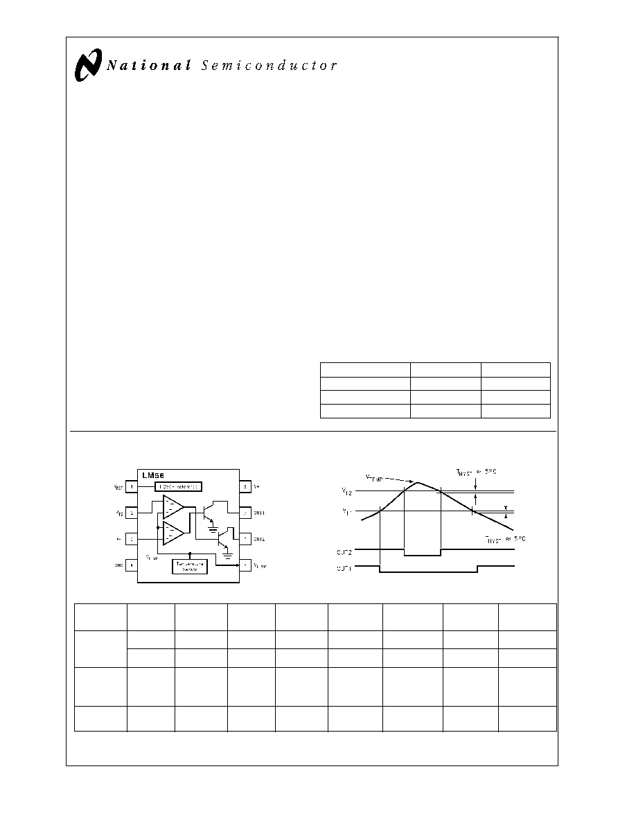
The LM56 is a precision low power thermostat. Two stable
temperature trip points (V
T1
and V
T2
) are generated by divid-
ing down the LM56 1.250V bandgap voltage reference using
3 external resistors. The LM56 has two digital outputs. OUT1
goes LOW when the temperature exceeds T1 and goes
HIGH when the the temperature goes below (T1T
HYST
).
Similarly, OUT2 goes LOW when the temperature exceeds
T2 and goes HIGH when the temperature goes below
(T2T
HYST
). T
HYST
is an internally set 5°C typical hysteresis.
The LM56 is available in an 8-lead Mini-SO8 surface mount
package and an 8-lead small outline package.
Applications
n
Microprocessor Thermal Management
n
Appliances
n
Portable Battery Powered 3.0V or 5V Systems
n
Fan Control
n
Industrial Process Control
n
HVAC Systems
n
Remote Temperature Sensing
n
Electronic System Protection
Features
n
Digital outputs support TTL logic levels
n
Internal temperature sensor
n
2 internal comparators with hysteresis
n
Internal voltage reference
n
Currently available in 8-pin SO plastic package
n
Future availability in the 8-pin Mini-SO8 package
Key Specifications
n
Power Supply Voltage
2.7V10V
n
Power Supply Current
230 µA (max)
n
V
REF
1.250V
±
1% (max)
n
Hysteresis Temperature
5°C
n
Internal Temperature Sensor
Output Voltage
(+6.20 mV/°C x T) +395 mV
n
Temperature Trip Point Accuracy:
LM56BIM
LM56CIM
+25°C
±
2°C (max)
±
3°C (max)
+25°C to +85°C
±
2°C (max)
±
3°C (max)
-40°C to +125°C
±
3°C (max)
±
4°C (max)
Simplified Block Diagram and Connection Diagram
Order
Number
LM56BIM
LM56BIMX
LM56CIM
LM56CIMX
LM56BIMM
LM56BIMMX
LM56CIMM
LM56CIMMX
NS
Package
Number
M08A
M08A
M08A
M08A
MUA08A
MUA08A
MUA08A
MUA08A
SOP-8
SOP-8
SOP-8
SOP-8
MSOP-8
MSOP-8
MSOP-8
MSOP-8
Transport
Media
2500 Units
2500 Units
3500 Units
3500 Units
Rail
Tape &
Reel
Rail
Tape &
Reel
Rail
Tape & Reel
Rail
Tape & Reel
Package
Marking
LM56BIM
LM56BIM
LM56CIM
LM56CIM
T02B
T02B
T02C
T02C
DS012893-1
DS012893-2
April 2000
LM56
Dual
Output
Low
Power
Thermostat
© 2000 National Semiconductor Corporation
DS012893
www.national.com
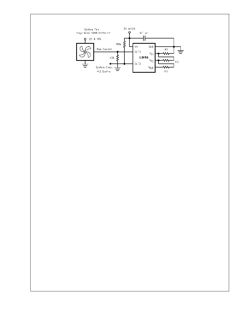
Typical Application
DS012893-3
V
T1
= 1.250V x (R1)/(R1 + R2 + R3)
V
T2
= 1.250V x (R1 + R2)/(R1 + R2 + R3)
where:
(R1 + R2 + R3) = 27 k
and
V
T1 or T2
= [6.20 mV/°C x T] + 395 mV therefore:
R1 = V
T1
/(1.25V) x 27 k
R2 = (V
T2
/(1.25V) x 27 k
) - R1
R3 = 27 k
- R1 - R2
FIGURE 1. Microprocessor Thermal Management
LM56
www.national.com
2

Absolute Maximum Ratings
(Note 1)
Input Voltage
12V
Input Current at any pin (Note 2)
5 mA
Package Input Current(Note 2)
20 mA
Package Dissipation at T
A
= 25°C
(Note 3)
900 mW
ESD Susceptibility (Note 4)
Human Body Model
1000V
Machine Model
200V
Soldering Information
SO Package (Note 5) :
Vapor Phase (60 seconds)
215°C
Infrared (15 seconds)
220°C
Storage Temperature
-65°C to + 150°C
Operating Ratings
(Note 1)
Operating Temperature Range
T
MIN
T
A
T
MAX
LM56BIM, LM56CIM
-40°C
T
A
+125°C
Positive Supply Voltage (V
+
)
+2.7V to +10V
Maximum V
OUT1
and V
OUT2
+10V
LM56 Electrical Characteristics
The following specifications apply for V
+
= 2.7 V
DC
, and V
REF
load current = 50 µA unless otherwise specified. Boldface lim-
its apply for T
A
= T
J
= T
MIN
to T
MAX
; all other limits T
A
= T
J
= 25°C unless otherwise specified.
Typical
LM56BIM
LM56CIM
Units
Symbol
Parameter
Conditions
(Note 6)
Limits
Limits
(Limits)
(Note 7)
(Note 7)
Temperature Sensor
Trip Point Accuracy (Includes
±
2
±
3
°C (max)
V
REF
, Comparator Offset, and
+25°C
T
A
+85°C
±
2
±
3
°C (max)
Temperature Sensitivity errors)
-40°C
T
A
+125°C
±
3
±
4
°C (max)
Trip Point Hysteresis
T
A
= -40°C
4
3
3
°C (min)
6
6
°C (max)
T
A
= +25°C
5
3.5
3.5
°C (min)
6.5
6.5
°C (max)
T
A
= +85°C
6
4.5
4.5
°C (min)
7.5
7.5
°C (max)
T
A
= +125°C
6
4
4
°C (min)
8
8
°C (max)
Internal Temperature
+6.20
mV/°C
Sensitivity
Temperature Sensitivity Error
±
2
±
3
°C (max)
±
3
±
4
°C (max)
Output Impedance
-1 µA
I
L
+40 µA
1500
1500
(max)
Line Regulation
+3.0V
V
+
+10V,
+25 ° C
T
A
+85 ° C
±
0.36
±
0.36
mV/V (max)
+3.0V
V
+
+10V,
-40 ° C
T
A
<
25 ° C
±
0.61
±
0.61
mV/V (max)
+2.7V
V
+
+3.3V
±
2.3
±
2.3
mV (max)
V
T1
and V
T2
Analog Inputs
I
BIAS
Analog Input Bias Current
150
300
300
nA (max)
V
IN
Analog Input Voltage Range
V
+
- 1
V
GND
V
V
OS
Comparator Offset
2
8
8
mV (max)
V
REF
Output
V
REF
V
REF
Nominal
1.250V
V
V
REF
Error
±
1
±
1
% (max)
±
12.5
±
12.5
mV (max)
V
REF
/
V
+
Line Regulation
+3.0V
V
+
+10V
0.13
0.25
0.25
mV/V (max)
+2.7V
V
+
+3.3V
0.15
1.1
1.1
mV (max)
V
REF
/
I
L
Load Regulation Sourcing
+30 µA
I
L
+50 µA
0.15
0.15
mV/µA
(max)
LM56
www.national.com
3

LM56 Electrical Characteristics
The following specifications apply for V
+
= 2.7 V
DC
, and V
REF
load current = 50 µA unless otherwise specified. Boldface lim-
its apply for T
A
= T
J
= T
MIN
to T
MAX
; all other limits T
A
= T
J
= 25°C unless otherwise specified.
Symbol
Parameter
Conditions
Typical
Limits
Units
(Note 6)
(Note 7)
(Limits)
V
+
Power Supply
I
S
Supply Current
V
+
= +10V
230
µA (max)
V
+
= +2.7V
230
µA (max)
Digital Outputs
I
OUT("1")
Logical "1" Output Leakage
V
+
= +5.0V
1
µA (max)
Current
V
OUT("0")
Logical "0" Output Voltage
I
OUT
= +50 µA
0.4
V (max)
Note 1: Absolute Maximum Ratings indicate limits beyond which damage to the device may occur. Operating Ratings indicate conditions for which the device is func-
tional, but do not guarantee specific performance limits. For guaranteed specifications and test conditions, see the Electrical Characteristics. The guaranteed speci-
fications apply only for the test conditions listed. Some performance characteristics may degrade when the device is not operated under the listed test conditions.
Note 2: When the input voltage (V
I
) at any pin exceeds the power supply (V
I
<
GND or V
I
>
V
+
), the current at that pin should be limited to 5 mA. The 20 mA maxi-
mum package input current rating limits the number of pins that can safely exceed the power supplies with an input current of 5 mA to four.
Note 3: The maximum power dissipation must be derated at elevated temperatures and is dictated by T
Jmax
(maximum junction temperature),
JA
(junction to am-
bient thermal resistance) and T
A
(ambient temperature). The maximum allowable power dissipation at any temperature is P
D
= (T
Jmax
T
A
)/
JA
or the number given
in the Absolute Maximum Ratings, whichever is lower. For this device, T
Jmax
= 125°C. For this device the typical thermal resistance (
JA
) of the different package
types when board mounted follow:
Package Type
JA
M08A
110°C/W
MUA08A
250°C/W
Note 4: The human body model is a 100 pF capacitor discharge through a 1.5 k
resistor into each pin. The machine model is a 200 pF capacitor discharged directly
into each pin.
Note 5: See AN450 "Surface Mounting Methods and Their Effects on Product Reliability" or the section titled "Surface Mount" found in any post 1986 National Semi-
conductor Linear Data Book for other methods of soldering surface mount devices.
Note 6: Typicals are at T
J
= T
A
= 25°C and represent most likely parametric norm.
Note 7: Limits are guaranteed to National's AOQL (Average Outgoing Quality Level).
LM56
www.national.com
4
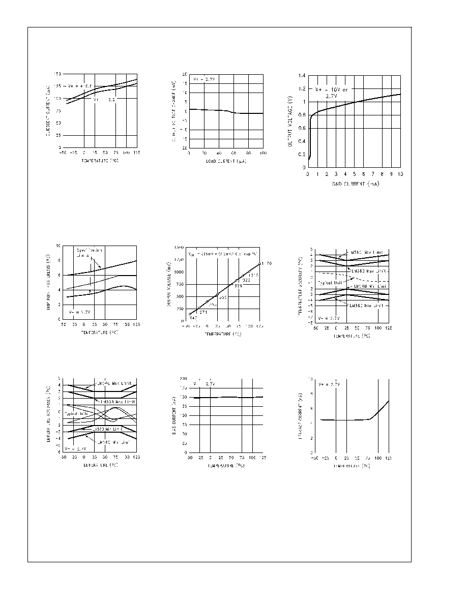
Typical Performance Characteristics
Quiescent Current vs
Temperature
DS012893-4
V
REF
Output Voltage vs
Load Current
DS012893-5
OUT1 and OUT2 Voltage
Levels vs Load Current
DS012893-32
Trip Point Hysteresis vs
Temperature
DS012893-7
Temperature Sensor
Output Voltage vs
Temperature
DS012893-8
Temperature Sensor
Output Accuracy vs
Temperature
DS012893-9
Trip Point
Accuracy vs Temperature
DS012893-10
Comparator Bias Current
vs Temperature
DS012893-11
OUT1 and OUT2 Leakage
Current vs Temperature
DS012893-12
LM56
www.national.com
5