LM556
Dual Timer
General Description
The LM556 Dual timing circuit is a highly stable controller ca-
pable of producing accurate time delays or oscillation. The
556 is a dual 555. Timing is provided by an external resistor
and capacitor for each timing function. The two timers oper-
ate independently of each other sharing only V
CC
and
ground. The circuits may be triggered and reset on falling
waveforms. The output structures may sink or source
200mA.
Features
n
Direct replacement for SE556/NE556
n
Timing from microseconds through hours
n
Operates in both astable and monostable modes
n
Replaces two 555 timers
n
Adjustable duty cycle
n
Output can source or sink 200mA
n
Output and supply TTL compatible
n
Temperature stability better than 0.005% per °C
n
Normally on and normally off output
Applications
n
Precision timing
n
Pulse generation
n
Sequential timing
n
Time delay generation
n
Pulse width modulation
n
Pulse position modulation
n
Linear ramp generator
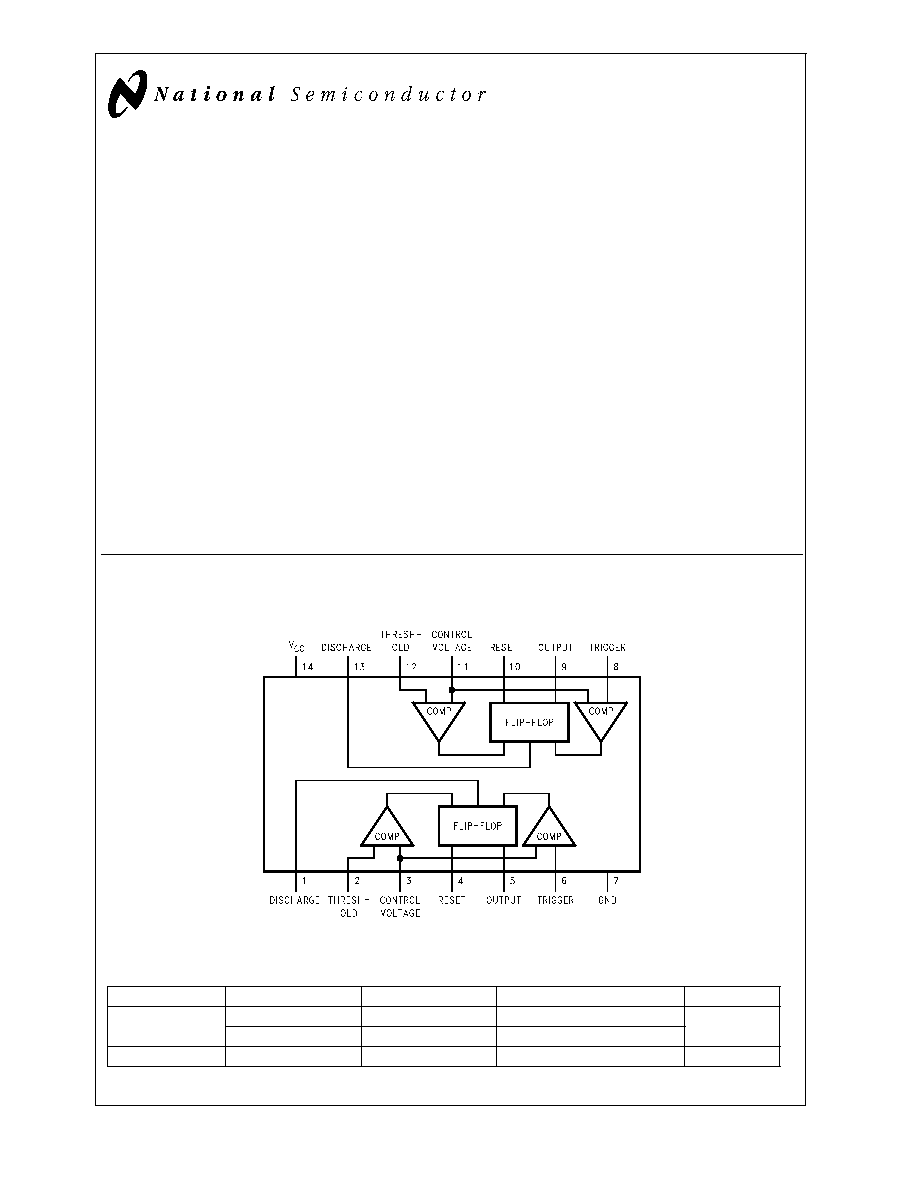
Connection Diagram
Ordering Information
Package
Part Number
Package Marking
Media Transport
NSC Drawing
14-Pin SOIC
LM556CM
LM556CM
Rails
M14A
LM556CMX
LM556CM
2.5k Units Tape and Reel
14-Pin MDIP
LM556CN
LM556CN
Rails
N14a
Dual-In-Line, Small Outline Packages
DS007852-1
Top View
March 2000
LM556
Dual
T
imer
© 2000 National Semiconductor Corporation
DS007852
www.national.com
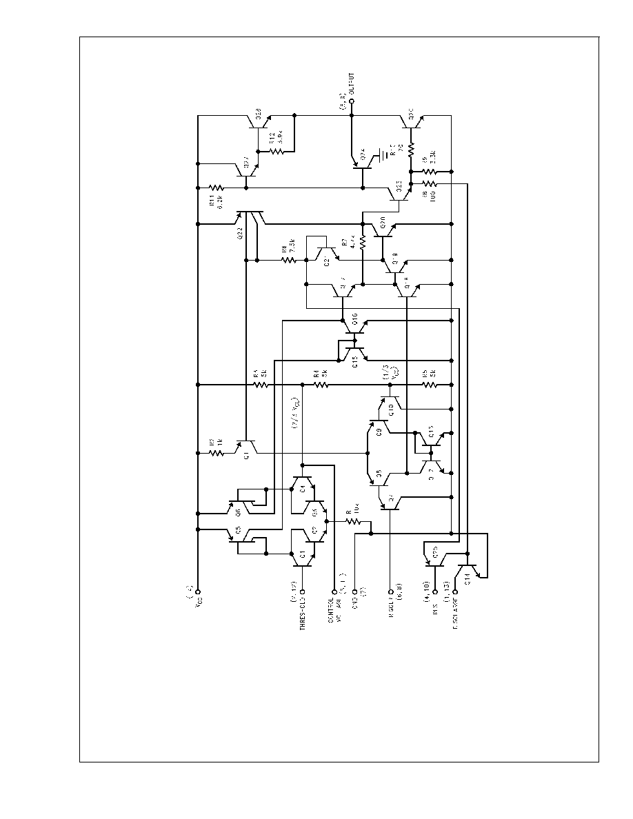
Schematic Diagram
DS007852-2
LM556
www.national.com
2
Absolute Maximum Ratings
(Note 1)
If Military/Aerospace specified devices are required,
please contact the National Semiconductor Sales Office/
Distributors for availability and specifications.
Supply Voltage
+18V
Power Dissipation (Note 2)
LM556CM
410 mW
LM556CN
1620 mW
Operating Temperature Ranges
LM556C
0°C to +70°C
Storage Temperature Range
-65°C to +150°C
Soldering Information
Dual-In-Line Package
Soldering (10 Seconds)
260°C
Small Outline Packages
Vapor Phase (60 Seconds)
215°C
Infrared (15 Seconds)
220°C
See AN-450 "Surface Mounting Methods and Their Effect
on Product Reliability" for other methods of soldering
surface mount devices.
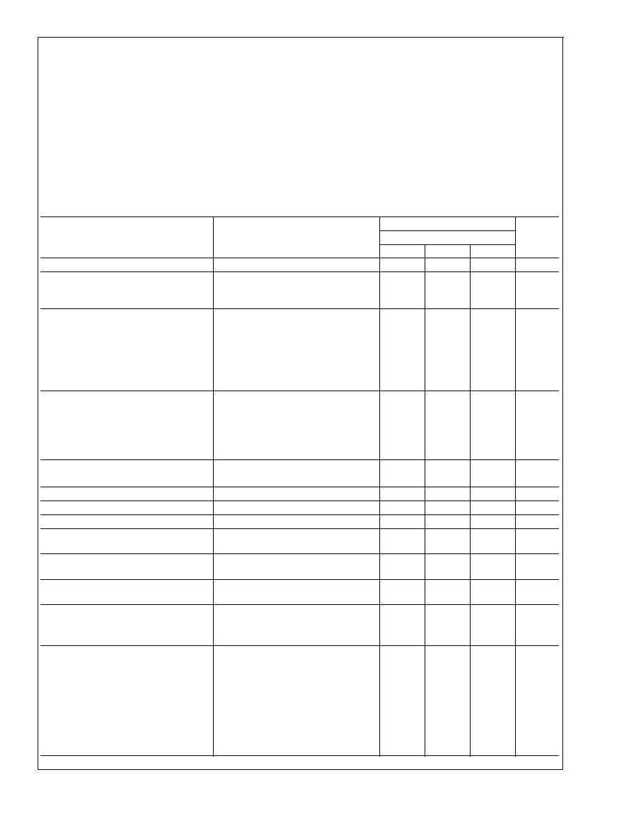
Electrical Characteristics
(T
A
= 25°C, V
CC
= +5V to +15V, unless otherwise specified)
Parameter
Conditions
Limits
Units
LM556C
Min
Typ
Max
Supply Voltage
4.5
16
V
Supply Current
(Each Timer Section)
V
CC
= 5V, R
L
=
V
CC
= 15V, R
L
=
(Low State) (Note 3)
3
10
6
14
mA
Timing Error, Monostable
Initial Accuracy
0.75
%
Drift with Temperature
R
A
= 1k to 100k
,
50
ppm/°C
C = 0.1µF, (Note 4)
Accuracy over Temperature
1.5
%
Drift with Supply
0.1
%/V
Timing Error, Astable
Initial Accuracy
2.25
%
Drift with Temperature
R
A
, R
B
= 1k to 100k
,
150
ppm/°C
Accuracy over Temperature
C = 0.1µF, (Note 4)
3.0
%
Drift with Supply
0.30
%/V
Trigger Voltage
V
CC
= 15V
4.5
5
5.5
V
V
CC
= 5V
1.25
1.67
2.0
V
Trigger Current
0.2
1.0
µA
Reset Voltage
0.4
0.5
1
V
Reset Current
0.1
0.6
mA
Threshold Current
V
TH
= V-Control (Note 6)
V
TH
= 11.2V
0.03
0.1
250
µA
nA
Control Voltage Level and
Threshold Voltage
V
CC
= 15V
V
CC
= 5V
9
2.6
10
3.33
11
4
V
Pin 1, 13
Leakage Output High
1
100
nA
Pin 1, 13 Sat
(Note 7)
Output Low
V
CC
= 15V, I = 15mA
180
300
mV
Output Low
V
CC
= 4.5V, I = 4.5mA
80
200
mV
Output Voltage Drop (Low)
V
CC
= 15V
I
SINK
= 10mA
0.1
0.25
V
I
SINK
= 50mA
0.4
0.75
V
I
SINK
= 100mA
2
2.75
V
I
SINK
= 200mA
2.5
V
V
CC
= 5V
I
SINK
= 8mA
V
I
SINK
= 5mA
0.25
0.35
V
LM556
www.national.com
3
Electrical Characteristics
(Continued)
(T
A
= 25°C, V
CC
= +5V to +15V, unless otherwise specified)
Parameter
Conditions
Limits
Units
LM556C
Min
Typ
Max
Output Voltage Drop (High)
I
SOURCE
= 200mA, V
CC
= 15V
12.5
V
I
SOURCE
= 100mA, V
CC
= 15V
12.75
13.3
V
V
CC
= 5V
2.75
3.3
V
Rise Time of Output
100
ns
Fall Time of Output
100
ns
Matching Characteristics
(Note 8)
Initial Timing Accuracy
0.1
2.0
%
Timing Drift with Temperature
±
10
ppm/°C
Drift with Supply Voltage
0.2
0.5
%/V
Note 1: Absolute Maximum Ratings indicate limits beyond which damage to the device may occur.
Note 2: For operating at elevated temperatures the device must be derated based on a +150°C maximum junction temperature and a thermal resistance of 77°C/W
(Plastic Dip), and 110°C/W (SO-14 Narrow).
Note 3: Supply current when output high typically 1mA less at V
CC
= 5V.
Note 4: Tested at V
CC
= 5V and V
CC
= 15V.
Note 5: As reset voltage lowers, timing is inhibited and then the output goes low.
Note 6: This will determine the maximum value of R
A
+ R
B
for 15V operation. The maximum total (R
A
+ R
B
) is 20 M
.
Note 7: No protection against excessive pin 1, 13 current is necessary providing the package dissipation rating will not be exceeded.
Note 8: Matching characteristics refer to the difference between performance characteristics of each timer section.
Note 9: Refer to RETS556X drawing of military LM556J versions.
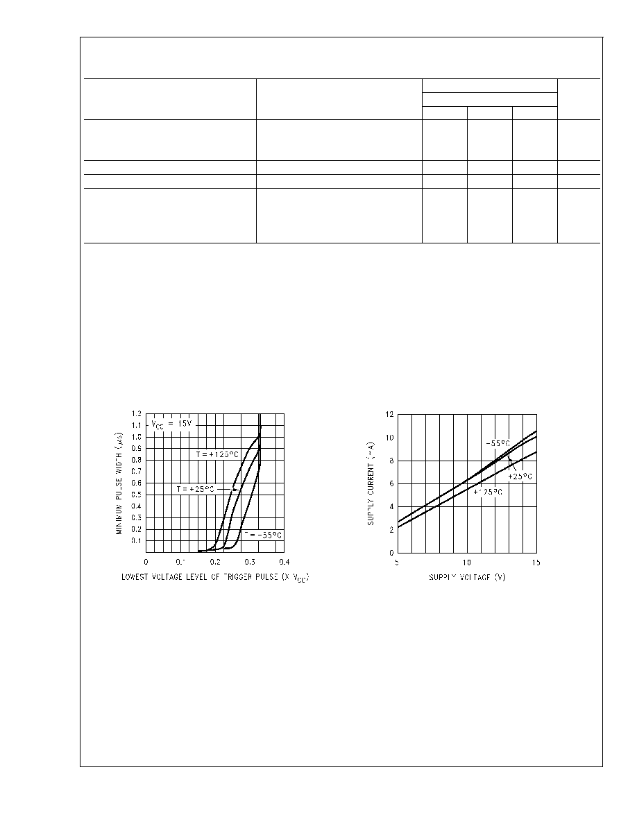
Typical Performance Characteristics
Minimum Pulse Width Required for Triggering
DS007852-3
Supply Current vs. Supply Voltage (Each Section)
DS007852-4
LM556
www.national.com
4
Typical Performance Characteristics
(Continued)
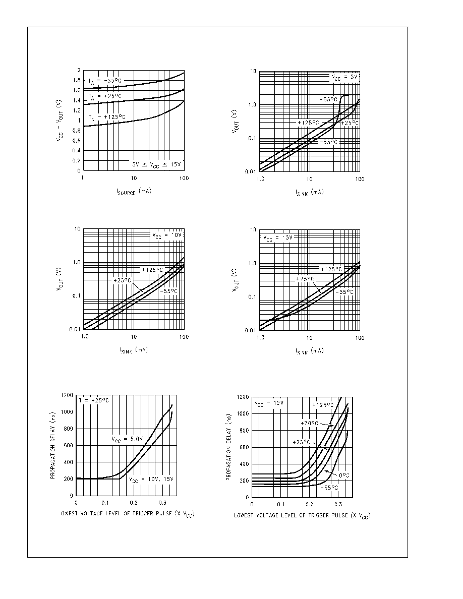
High Output Voltage vs. Output Source Current
DS007852-5
Low Output Voltage vs. Output Sink Current
DS007852-6
Low Output Voltage vs. Output Sink Current
DS007852-7
Low Output Voltage vs. Output Sink Current
DS007852-8
Output Propagation Delay vs. Voltage Level of Trigger
Pulse
DS007852-9
Output Propagation Delay vs. Voltage Level of Trigger
Pulse
DS007852-10
LM556
www.national.com
5