
LM3658
Dual Source USB/AC Li Chemistry Charger IC for
Portable Applications
General Description
The LM3658 is a single chip charger IC designed for hand-
held applications. It can safely charge and maintain a single
cell Li-Ion/Polymer battery operating from an AC wall
adapter or USB power source. Input power source selection
of USB/AC is automatic. With both power sources present,
the AC power source has priority. Charge current is pro-
grammed through an external resistor when operating from
an AC wall adapter allowing charge currents from 50 mA to
1000 mA. When the battery is charged using USB power,
charge currents of 100 mA or 500 mA are pin-selectable. The
termination voltage is controlled to within
±
0.35% of 4.2V.
The LM3658 requires few external components and inte-
grates internal power FETs, reverse current protection and
current sensing. The internal power FETs are thermally regu-
lated to obtain the most efficient charging rate for a given
ambient temperature.
The LM3658 operates in five modes: pre-qualification mode,
constant-current mode, constant-voltage mode, top-off
mode and maintenance mode. Optimal battery management
is obtained through thermal regulation, battery temperature
measurement and multiple safety timers. The LM3658 pro-
vides two open-drain outputs for LED status indication or
connection to GPIOs.
Features
n
Integrated power FETs with thermal regulation
n
Charges from either an AC wall adapter or USB power
source with automatic source selection
n
50 mA to 1000 mA charge currents using AC wall
adapter
n
Pin-selectable USB charge currents of 100 mA or
500 mA
n
Continuous battery temperature monitoring
n
Built-in multiple safety timers
n
Charge status indication
n
Continuous over-current and temperature protection
n
Near-depleted battery pre-conditioning
n
Sleep mode with ultra low quiescent current
n
On-board Kelvin-sensing achieves
±
0.35% termination
accuracy
n
Maintenance mode with automatic recharge
n
Thermally enhanced 3 mm x 3 mm LLP package
Applications
n
Smartphones
n
Digital still cameras
n
PDAs
n
Hard Drive and flash-based MP3 players
n
USB-powered devices
Typical Application
20128201
May 2005
LM3658
Dual
Source
USB/AC
Li
Chemistry
Charger
IC
for
Portable
Applications
© 2005 National Semiconductor Corporation
DS201282
www.national.com

Connection Diagram and Package Mark Information
LLP10 Package Drawing
20128202
Note: The actual physical placement of the package marking will vary from part to part. The package marking "X" is the manufacturing plant code. "YY" is a
2-digit date code, and "ZZ" for die traceability. These codes will vary considerably. "L111B" identifies the device (part number, option, etc.).
TABLE 1. LM3658 Pin Description
Pin #
Name
Description
1
CHG_IN
AC wall adapter input pin.
2
USBpwr
USB power input pin.
3
GND
Power and signal ground pin.
4
USB_sel
Pulling this pin low limits the USB charge current to 100 mA. Pulling this pin high limits the USB
charge current to 500 mA.
5
EN_b
Pulling this pin low enables the charger. Pulling this pin high disables the charger.
6
STAT2
Active low open-drain output. Indicates charger status. This pin is capable of driving an LED as well
as GPIOs. See Operation Description section for more detail.
7
STAT1
Active low open-drain output. Indicates charger status. This pin is capable of driving an LED as well
as GPIO. See Operation Description section for more detail.
8
I
SET
A resistor is connected between this pin and GND. The resistor value determines the full-rate charge
current when using the AC source.
9
T
S
Battery temperature sense pin. This pin must be connected to battery pack's temperature sense
output pin. See Operation Description section for more detail.
10
BATT
Positive battery terminal connection.
TABLE 2. Ordering Information
Order Number
Package
Marking
Supplied As
LM3658SD
L111B
1000 units, Tape-and-Reel
LM3658SDX
L111B
4500 units, Tape-and-Reel
For more information on the various options, please refer to Operation Description section.
LM3658
www.national.com
2

Absolute Maximum Ratings
(Notes 1,
2)
If Military/Aerospace specified devices are required,
please contact the National Semiconductor Sales Office/
Distributors for availability and specifications.
CHG_IN, USBpwr (V
CC
)
-0.3V to +6.5V
All other pins except GND
-0.3V to CHG_IN or USBpwr
Power Dissipation (Note 3)
Internally Limited
Junction Temperature (T
J-MAX)
+150°C
Storage Temperature Range
-65°C to +150°C
ESD Rating (Note 4)
Human Body Model:
Machine Model:
2.0 kV
200V
Operating Ratings
(Notes 1, 2)
Input Voltage Range for CHG_IN
4.5V to 6.0V
Input Voltage Range for USB_pwr
4.35V to 6.0V
Recommended Load Current
0 to 1000 mA
Power Dissipation(Note 3)
Internally Limited
Junction Temperature (T
J
) Range
-40°C to +125°C
Ambient Temperature (T
A
) Range
-40°C to +85°C
Thermal Properties
JA
, Junction-to-Ambient Thermal
54°C/W
Resistance (Note 5)
Electrical Characteristics
Unless otherwise noted, V
CC
(V
CHG_IN
and/or V
USBpwr
) = 5V, V
BATT
= 3.5V.
C
CHG_IN
= 1 µF, C
USBpwr
= 1 µF, C
BATT
= 1 µF. Typical values and limits appearing in normal type apply for T
J
= 25°C. Limits
appearing in boldface type apply over T
J
= 0°C to +85°C. (Notes 2, 6, 7)
Symbol
Parameter
Conditions
Typ
Limit
Units
Min
Max
CHARGER
V
CHG_IN
AC Wall Adapter
Input Voltage Range
4.5
6.0
V
V
USBpwr
USB Input Voltage
Range
4.35
6.0
V
I
CC_PD
Quiescent Current in
Power Down Mode
V
BATT
>
V
CC
V
OK_CHG
1
5
µA
I
CC_STBY
Quiescent Current in
Standby Mode
V
BATT
<
V
CC
- V
OK_CHG
V
CC
>
V
POR
EN_b = High
400
600
µA
I
BATT_PD
Battery Leakage
Current in Power
Down Mode
V
BATT
>
V
CC
+ V
OK_CHG
0.01
2.0
µA
I
BATT_MAINT
Battery Leakage
Current in
Maintenance Mode
STAT1 = off, STAT2 = on, adapter or USB
connected, V
BATT
= 4.2V
7
15
µA
V
OK_CHG
CHG_IN or USBpwr
OK Trip-Point
V
CC
V
BATT
(Rising)
V
CC
V
BATT
(Falling)
200
50
mV
V
POR
V
CC
POR Trip-Point
V
CC
(Rising)
V
BATT
<
V
CC
V
OK_CHG
V
FULL_RATE
<
V
BATT
<
V
TERM
3.0
V
V
TERM
Battery Charge
Termination Voltage
I
CHG
= 10% of its value when V
BATT
= 3.5V
4.2
V
Battery Charge
Termination Voltage
Tolerance
T
A
= 25°C
-0.35
+0.35
%
T
A
= 0°C to 85°C
-1.5
+1.5
V
CHG_DO
CHG_IN Drop-Out
Voltage
V
BATT
= V
TERM
, I
CHG
= 1A
V
CC
>
V
BATT
+ V
CHG_DO_MAX
500
mV
V
USB_DO
USBpwr Drop-Out
Voltage
V
BATT
= V
TERM
, USB_sel = high
V
CC
>
V
BATT
+ V
USB_DO_MAX
250
mV
I
CHG
CHG_IN Full-Rate
Charge Current
Range (see full-rate
charge mode
description)
6V
V
CC
4.5V
V
BATT
<
V
CC
V
OK_CHG
V
FULL_RATE
<
V
BATT
<
V
TERM
I
CHG
= K
ISET
/R
ISET
50
1000
mA
LM3658
www.national.com
3

Electrical Characteristics
Unless otherwise noted, V
CC
(V
CHG_IN
and/or V
USBpwr
) = 5V, V
BATT
= 3.5V.
C
CHG_IN
= 1 µF, C
USBpwr
= 1 µF, C
BATT
= 1 µF. Typical values and limits appearing in normal type apply for T
J
= 25°C. Limits
appearing in boldface type apply over T
J
= 0°C to +85°C. (Notes 2, 6, 7) (Continued)
Symbol
Parameter
Conditions
Typ
Limit
Units
Min
Max
CHARGER
I
CHG
CHG_IN Full Rate
Charge Current
R
ISET
= 10k
245
220
270
mA
R
ISET
= 5 k
500
465
535
R
ISET
= 3.3k
760
700
820
K
ISET
Charge Current Set
Coefficient
I
CHG
= K
ISET
/R
ISET
(see full-rate charge
mode description)
6V
V
CC
4.5V
V
BATT
<
V
CC
V
OK_CHG
V
FULL_RATE
<
V
BATT
<
V
TERM
2500
A
V
ISET
Charge Current Set
Voltage
6V
V
CC
4.5V
V
BATT
<
V
CC
V
OK_CHG
V
FULL_RATE
<
V
BATT
<
V
TERM
2.5
V
I
USB_L
USB Full-Rate
Charge Low Current
90
80
100
mA
I
USB_H
USB Full-Rate
Charge High Current
450
400
500
mA
I
PREQUAL
Pre-Qualification
Current
V
BATT
= 2V, for both AC adapter and USB
45
35
55
mA
V
FULL_RATE
Full-Rate
Qualification
Threshold
V
BATT
rising, transition from pre-qualification to
full-rate charging
3.0
2.9
3.1
V
Full Rate Hysteresis
V
BATT
falling
60
50
70
mV
I
EOC
End-of-Charge
Current, Percent from
Full-Range Current
6V
V
CC
4.5V
V
BATT
<
V
CC
V
OK_CHG
V
FULL_RATE
<
V
BATT
<
V
TERM
9
7
11
%
I
TOPOFF
Minimum Top-Off
Charge Current
6V
V
CC
4.5V
V
BATT
<
V
CC
V
OK_CHG
V
BATT
= V
TERM
2.5
1.25
3.75
%
V
RESTART
Restart Threshold
Voltage
V
BATT
falling, transition from EOC to
pre-qualification mode
4.0
3.94
4.07
V
V
TL
Battery Temperature
Sense Comparator
Low-Voltage
Threshold
0.49
0.46
0.52
V
V
TH
Battery Temperature
Sense Comparator
High-Voltage
Threshold
2.49
2.44
2.54
V
I
TSENSE
Battery Temperature
Sense Current
100
94
106
µA
T
REG
Regulated Junction
Temperature
120
°C
T
SD
Thermal Shutdown
Temperature
165
°C
DETECTION AND TIMING
T
POK
Power OK Deglitch
Time
V
BATT
<
V
CC
V
OK_CHG
60
40
100
ms
T
PREQUAL
Pre-Qualification
Timer
30
27
33
mins
LM3658
www.national.com
4

Electrical Characteristics
Unless otherwise noted, V
CC
(V
CHG_IN
and/or V
USBpwr
) = 5V, V
BATT
= 3.5V.
C
CHG_IN
= 1 µF, C
USBpwr
= 1 µF, C
BATT
= 1 µF. Typical values and limits appearing in normal type apply for T
J
= 25°C. Limits
appearing in boldface type apply over T
J
= 0°C to +85°C. (Notes 2, 6, 7) (Continued)
Symbol
Parameter
Conditions
Typ
Limit
Units
Min
Max
DETECTION AND TIMING
T
PQ_FULL
Deglitch Time for
Pre-Qualification to
Full-Rate Charge
Transition
300
270
330
ms
T
FULL_PQ
Deglitch Time for
Full-Rate to
Pre-Qualification
Transition
300
270
330
ms
T
CHG
Charge Timer
300
270
330
min
T
EOC
Deglitch Time for
End-of-Charge
Transition
300
270
330
ms
T
BATTEMP
Deglitch Time for
Battery Temperature
Fault
40
20
80
ms
T
DGL
Deglitch Time for
EN_b and USB_sel
Pins
40
20
80
ms
T
ITOPOFF
Deglitch Time for
I
TOPOFF
300
270
330
ms
T
TOPOFF
Top-Off Charging
Timer
30
27
33
min
I/O
V
IL
Low-Level Input
Voltage
EN_b
0
0.7
V
USB_sel
1.5
V
IH
High-Level Input
Voltage
EN_b
1.4
V
USB_sel
2.5
I
OL
Low-Level Output
Current
STAT1, STAT2, output voltage = 0.25V
25
10
mA
I
OH
High-Level Output
Current
STAT1, STAT2, output voltage = 6.0V
0.01
1
µA
Note 1: Absolute Maximum Ratings indicate limits beyond which damage to the component may occur. Operating Ratings are conditions under which operation of
the device is guaranteed. Operating Ratings do not imply guaranteed performance limits. For guaranteed performance limits and associated test conditions, see the
Electrical Characteristics tables.
Note 2: All voltages are with respect to the potential at the GND pin.
Note 3: The LM3658 has built-in thermal regulation to regulate the die temperature to 120
o
C. See Operation Description section for more detail.
Note 4: The Human body model is a 100 pF capacitor discharged through a 1.5 k
resistor into each pin. The machine model is a 200 pF capacitor discharged
directly into each pin. MIL-STD-883 3015.7
Note 5: Junction-to-ambient thermal resistance is highly application and board-layout dependent. In applications where high maximum power dissipation exists,
special care must be paid to thermal dissipation issues in board design. Please refer to application note AN1187 for more detail.
Note 6: Min and Max limits are guaranteed by design, test, or statistical analysis. Typical numbers are not guaranteed, but do represent the most likely norm.
Note 7: LM3658 is not intended as a Li-Ion battery protection device; battery used in this application should have an adequate internal protection.
LM3658
www.national.com
5

Block Diagram
20128203
LM3658
www.national.com
6

Li-Ion Charging Profile
20128204
LM3658
www.national.com
7

LM3658 Operation Description
POWER-DOWN MODE
The LM3658 will power down automatically when the voltage
on the USBpwr or CHG_IN pin drops below the battery
voltage with an amount that is equal to V
OK_CHG
(V
BATT
>
V
CC
- V
OK_CHG
). Power-Down mode shuts off the internal
power FETs as well as the open-drain pull-down transistors
on the status pins STAT1 and STAT2. The only current
consumed by the LM3658 is an ultra-low quiescent current
of 1 µA typical.
POWER-ON RESET
As soon as the voltage of one of the power sources rises
above V
BATT
+ V
OK_CHG
, the charger will wake up. However,
charging will not be initiated unless the supply voltage
source exceeds the V
POR
.
AUTOMATIC POWER SOURCE DETECTION
When the voltage of one of the power sources exceeds the
V
POR
threshold, the LM3658 detects which power source is
a valid charge supply. When both supply voltages are valid
and present, CHG_IN will automatically be selected over
USBpwr. The USBpwr will be the designated power source
only if no CHG_IN is present or when the voltage on the
CHG_IN pin is less than the battery voltage.
THERMAL POWER FET REGULATION
The internal power FETs are thermally regulated to the junc-
tion temperature of 120
o
C to guarantee optimal charging of
the battery. At all times is the charge current limited by the
I
SET
resistor setting, the USB 100 mA/500 mA selection, or
the 100
o
C junction temperature of the LM3658. The charge
current is therefore a function of the charge current settings,
the thermal conductivity of the package and the ambient
temperature as described in the following equation:
20128205
Where T
A
is the ambient temperature and
JA
is the thermal
resistance of the package. Thermal regulation guarantees
maximum charge current and superior charge rate without
exceeding the power dissipation limits of the LM3658.
PRE-QUALIFICATION MODE
During pre-qualification, STAT1 is on and STAT2 is off, and
the charger supplies a constant current of 50 mA to the
battery. When the battery voltage reaches V
FULL_RATE
, the
charger transitions from pre-qualification to full-rate charg-
ing. The pre-qualification mode aborts when the battery
doesn't reach V
FULL_RATE
within the time allowed in
T
PREQUAL
timer. In this event, charging stops and STAT1 and
STAT2 will both be on, indicating a bad battery condition.
CHG_IN FULL-RATE CHARGING MODE
The full-rate charge cycle is initiated following the successful
completion of the pre-qualification mode. Timer T
CHG
starts
to count when the charger enters full-rate charging, with
STAT1 on and STAT2 off. When charging with an AC wall
adapter, the full-rate charge current is proportional to the
value of the resistor that is connected to the I
SET
pin as
described in the following equation:
It is recommended to charge Li-Ion batteries at 1C rate,
where "C" is the capacity of the battery. As an example, it is
recommended to charge a 750 mAh battery at 750 mA, or
1C. Charging at a higher rate can cause damage to the
battery.
USBpwr FULL-RATE CHARGING MODE
The full-rate charge cycle is initiated following the successful
completion of the pre-qualification mode. Timer T
CHG
starts
to count when the charger enters full-rate charging, with
STAT1 on and STAT2 off. If the USB bus provides the
charger supply, then the default full-rate charge current is
100 mA max unless the USB_sel pin is pulled high, which
sets the charge current to 500 mA max.
CONSTANT-VOLTAGE CHARGING MODE AND
END-OF-CHARGE (EOC) DETECTION
The battery voltage increases rapidly as a result of full-rate
charging and will reach the 4.2V termination voltage, trigger-
ing the constant-voltage charge cycle. Timer T
CHG
continues
to count in this cycle. STAT1 is on and STAT2 is off. The
charge current gradually decreases during constant-voltage
charging until it reaches the End-Of-Charge (EOC), which is
equal to 10% of the full-rate current set either by the resistor
connected to the I
SET
pin or the USB_sel pin. If Timer T
CHG
times out before EOC is reached, charging stops and STAT1
and STAT2 will both be on, indicating a bad battery condition.
TOP-OFF CHARGING MODE
Once EOC has been reached, a top-off cycle continues to
charge the battery. Timed top-off cycle provides optimal
battery capacity following a complete charge cycle. During
this cycle, charging terminates when I
CHG
reaches 2.5% of
the full-rate charge current or when T
TOPOFF
times out,
whichever occurs first. STAT1 will turn off and STAT2 will turn
on once the top-off cycle completes successfully, indicating
that charging is done.
MAINTENANCE MODE
Maintenance mode begins immediately after the charger
successfully finishes the top-off cycle. In the maintenance
mode, the battery voltage is being monitored by the LM3658
continuously. If the battery voltage drops 200 mV below
V
TERM
, a new full-rate charge cycle starts to replenish the
battery. As this new full-rate charge cycle begins, STAT1 will
turn on and STAT2 will turn off, and all the timers will reset.
Refer to the LM3658 Flowchart.
CHARGE STATUS OUTPUTS
The LM3658 provides two open-drain outputs STAT1 and
STAT2 that can be connected to external LEDs or to General
Purpose I/O's (GPIO) of a peripheral IC. All charge status of
the LM3658 is illustrated in Table 3. "ON" means that STATx
pin is pulled low as its pull-down transistor is turned on,
representing a logic 0.
LM3658
www.national.com
8

LM3658 Operation Description
(Continued)
TABLE 3. Status Pins Summary
STAT1
STAT2
Condition
OFF
OFF
Power-Down, charging is
suspended or interrupted
ON
OFF
Pre-qualification mode, CC and CV
charging, Top-off mode
OFF
ON
Charge is completed
ON
ON
Bad battery (Safety timer expired),
or LDO mode
SAFETY TIMERS
In order to prevent endless charging of the battery, which
can cause damage to the battery, there are three safety
timers that forcefully terminate charging if the charging mode
is not completed within the time allowed.
Pre-Qualification Timer (T
PREQUAL
)
The pre-qualification timer starts with the initiation of the
pre-qualification mode and allows 30 minutes to transition
from pre-qualification to full rate charging. If the battery
voltage does not reach V
FULL_RATE
in 30 minutes, charging
stops and status pins STAT1 and STAT2 both turn on to
indicate a bad battery status.
Charger Timer (T
CHG
)
The charge timer starts with the initiation of full-rate charging
and has a duration of 5 hours for the LM3658. If the charge
current does not reach EOC, charging stops and STAT1 and
STAT2 both turn on to indicate a bad battery status. Once
the charge control declares a bad battery, removing the input
source is the only means to clear the bad battery status.
Top-Off Timer (T
TOPOFF
)
Once the charger successfully completes constant current
constant voltage charging, it enters top-off mode and starts
T
TOPOFF
timer. Topoff lasts 30 minutes for the LM3658.
During top-off, charging stops when T
TOPOFF
reaches its
count or when I
CHG
reaches 2.5% of the full-rate charge
current. There is no time-out condition in top-off mode.
When charging is interrupted either by battery temperature
out of range or disabling the LM3658, the applicable safety
timer will store its count value for the duration of the inter-
ruption and subsequently resumes counting from its stored
count value when charging continues, only if the charger
resumes to the same operation mode it was in before the
interrupt.
BATTERY TEMPERATURE MONITORING (Suspend
Mode)
The LM3658 is equipped with a battery thermistor interface
to continuously monitor the battery temperature by measur-
ing the voltage between the T
S
pin and ground. Charging is
allowed only if the battery temperature is within the accept-
able temperature range set by a pair of internal comparators
inside the LM3658. If the battery temperature is out of range,
STAT1 and STAT2 both turn off and charging is suspended.
Timer holds its count value.
The TS pin is only active during charging and draws no
current from the battery when no external power source is
present.
If the TS pin is not used in the application, it should be
connected to GND through 10k
pulldown resistor.
When the TS pin is left floating (battery removal), then the
charger will be disabled as the TS voltage exceeds the upper
temperature limit.
20128210
The LM3658 battery temperature feature is tailored to use
negative temperature coefficient (NTC) 103AT thermistors
with 10k
impedance. If alternative thermistors need to be
used in the system, supplemental external resistors are
needed to create a circuit with equivalent impedance.
20128211
DISABLING CHARGER (Charge Interrupt Mode)
Charging can be safely interrupted by pulling the EN_b pin
high and charging can resume upon pulling the EN_b pin
low. The enable pin can be permanently tied to GND with no
extra current consumption penalty during power down mode.
When the charger is disabled, timer holds its count value,
and STAT1 and STAT2 are both off.
INPUT/OUTPUT BYPASS CAPACITORS
Care should be taken to support the stability of the charge
system by connecting a 1 µF capacitor as close as possible
to the BATT pin. An input capacitor ranging from 1.0 µF
10.0 µF must be connected to the CHG_IN and USBpwr
input pins. Low cost ceramic capacitors can be selected.
THERMAL PERFORMANCE OF THE LLP PACKAGE
The LM3658 is a monolithic device with integrated power
FETs. For that reason, it is important to pay special attention
to the thermal impedance of the LLP package and to the
PCB layout rules in order to maximize power dissipation of
the LLP package.
The LLP package is designed for enhanced thermal perfor-
mance and features an exposed die attach pad at the bottom
center of the package that creates a direct path to the PCB
for maximum power dissipation. Compared to the traditional
leaded packages where the die attach pad is embedded
inside the molding compound, the LLP reduces one layer in
the thermal path.
LM3658
www.national.com
9

LM3658 Operation Description
(Continued)
The thermal advantage of the LLP package is fully realized
only when the exposed die attach pad is soldered down to a
thermal land on the PCB board with thermal vias planted
underneath the thermal land. Based on thermal analysis of
the LLP package, the junction-to-ambient thermal resistance
(
JA
) can be improved by a factor of two when the die attach
pad of the LLP package is soldered directly onto the PCB
with thermal land and thermal vias, as opposed to an alter-
native with no direct soldering to a thermal land. Typical pitch
and outer diameter for thermal vias are 1.27 mm and
0.33 mm respectively. Typical copper via barrel plating is 1
oz, although thicker copper may be used to further improve
thermal performance. The LM3658 die attach pad is con-
nected to the substrate of the IC and therefore, the thermal
land and vias on the PCB board need to be connected to
ground (GND pin).
For more information on board layout techniques, refer to
Application Note 1187 "Leadless Lead Frame Package
(LLP)." This application note also discusses package han-
dling, solder stencil and the assembly process.
LM3658
www.national.com
10

LM3658 Operation Description
(Continued)
20128207
LM3658 Flowcart
LM3658
www.national.com
11

LM3658 Operation Description
(Continued)
20128206
LM3658 USBpwr Mode Flowcart
20128208
LM3658 CHG_IN Mode Flowcart
LM3658
www.national.com
12
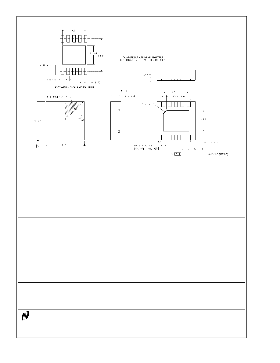
Physical Dimensions
inches (millimeters) unless otherwise noted
LLP10 Package Drawing
NS Package Number SDA10A
National does not assume any responsibility for use of any circuitry described, no circuit patent licenses are implied and National reserves
the right at any time without notice to change said circuitry and specifications.
For the most current product information visit us at www.national.com.
LIFE SUPPORT POLICY
NATIONAL'S PRODUCTS ARE NOT AUTHORIZED FOR USE AS CRITICAL COMPONENTS IN LIFE SUPPORT DEVICES OR SYSTEMS
WITHOUT THE EXPRESS WRITTEN APPROVAL OF THE PRESIDENT AND GENERAL COUNSEL OF NATIONAL SEMICONDUCTOR
CORPORATION. As used herein:
1. Life support devices or systems are devices or systems
which, (a) are intended for surgical implant into the body, or
(b) support or sustain life, and whose failure to perform when
properly used in accordance with instructions for use
provided in the labeling, can be reasonably expected to result
in a significant injury to the user.
2. A critical component is any component of a life support
device or system whose failure to perform can be reasonably
expected to cause the failure of the life support device or
system, or to affect its safety or effectiveness.
BANNED SUBSTANCE COMPLIANCE
National Semiconductor manufactures products and uses packing materials that meet the provisions of the Customer Products
Stewardship Specification (CSP-9-111C2) and the Banned Substances and Materials of Interest Specification (CSP-9-111S2) and contain
no ``Banned Substances'' as defined in CSP-9-111S2.
Leadfree products are RoHS compliant.
National Semiconductor
Americas Customer
Support Center
Email: new.feedback@nsc.com
Tel: 1-800-272-9959
National Semiconductor
Europe Customer Support Center
Fax: +49 (0) 180-530 85 86
Email: europe.support@nsc.com
Deutsch Tel: +49 (0) 69 9508 6208
English
Tel: +44 (0) 870 24 0 2171
Français Tel: +33 (0) 1 41 91 8790
National Semiconductor
Asia Pacific Customer
Support Center
Email: ap.support@nsc.com
National Semiconductor
Japan Customer Support Center
Fax: 81-3-5639-7507
Email: jpn.feedback@nsc.com
Tel: 81-3-5639-7560
www.national.com
LM3658
Dual
Source
USB/AC
Li
Chemistry
Charger
IC
for
Portable
Applications