LM3557
Step-Up Converter for White LED Applications
General Description
The LM3557 is a complete solution for white LED drive
applications. With minimal external component count, no DC
current leakage paths to ground, cycle-by-cycle current limit
protection, and output over-voltage protection circuitry, the
LM3557 offer superior performance and cost savings over
standard DC/DC boost component implementations.
The LM3557 switches at a fixed-frequency of 1.25 MHz,
which allows for the use of small external components. Also,
the LM3557 has a wide input voltage range to take advan-
tage of multi-cell input applications. With small external com-
ponents, high fixed frequency operation, and wide input
voltage range, the LM3557 is the most optimal choice for
LED lighting applications.
Features
n
V
IN
Range: 2.7V7.5V
n
Small External Components
n
1.25 MHz Constant-Switching Frequency
n
Output Over-Voltage Protection
n
Input Under-Voltage Protection
n
Cycle-By-Cycle Current Limit
n
TRUE SHUTDOWN: No DC current paths to ground
during shutdown
n
Low Profile Package:
<
1 mm Height -8 Pin LLP
n
No External Compensation
Applications
n
White LED Display Lighting
n
Cellular Phones
n
PDAs
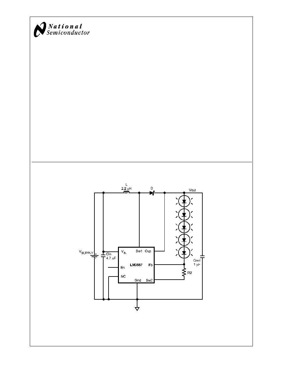
Typical Application Circuit
20131601
FIGURE 1. Backlight Configuration
November 2004
LM3557
Step-Up
Converter
for
White
LED
Applications
© 2004 National Semiconductor Corporation
DS201316
www.national.com

Connection Diagram
Top View
20131602
8-Lead Thin Leadless Leadframe Package
See NS Package Number SDA08A
Ordering Information
Order Number
Package
Marking
Supplied As
LM3557SD-2
L147B
1k Units, Tape and Reel
LM3557SDX-2
L147B
4.5k Units, Tape and Reel
Pin Description
Pin #
Name
Description
1
Sw1
Drain Connection of the Internal Power Field Effect Transistor (FET) Switch (Figure 2: N1)
2
V
IN
Input Voltage Connection
3
NC
No Connection
4
En
Device Enable Connection
5
Ovp
Over-Voltage Protection Input Connection
6
Fb
Feedback Voltage Connection
7
Sw2
Drain Connection of an Internal Field Effect Transistor (FET) Switch (Figure 2: N2)
8
Gnd
Ground Connection
DAP
DAP
Die Attach Pad (DAP), must be soldered to the printed circuit board's ground plane for enhanced thermal
dissipation
LM3557
www.national.com
2

Absolute Maximum Ratings
(Note 1)
If Military/Aerospace specified devices are required,
please contact the National Semiconductor Sales Office/
Distributors for availability and specifications.
V
IN
Pin
-0.3V to +8V
En Pin
-0.3V to +8V
Fb Pin
-0.3V to +8V
Sw2 Pin
-0.3V to +8V
Ovp Pin
-0.3V to +30V
Sw1 Pin
-0.3V to +40V
Continuous Power Dissipation
Internally Limited
Maximum Junction Temperature
(T
J-MAX
)
+150°C
Storage Temperature Range
-65°C to +150°C
ESD Rating (Note 2)
Human Body Model
Machine Model
2 kV
150V
Operating Conditions
(Notes 1, 6)
Junction Temperature (T
J
) Range
-40°C to +125°C
Ambient Temperature (T
A
) Range
-40°C to +85°C
Supply Voltage, V
IN
Pin
2.7V to 7.5V
En Pin
0V to V
IN
+0.4V
Thermal Properties
(Notes 4, 7)
Junction-to-Ambient Thermal
55°C/W
Resistance (
JA
), Leadless Leadframe Package
Electrical Characteristics
(Notes 6, 8) Limits in standard typeface are for T
J
= 25°C. Limits in bold type-
face apply over the full operating junction temperature range (-40°C
T
J
+125°C). Unless otherwise specified: V
IN
= 3.6V.
Symbol
Parameter
Conditions
Min
Typ
Max
Units
V
IN
Input Voltage
2.7
7.5
V
I
Q
Quiescent Current
V
EN
= 0V (Shutdown)
V
EN
= 1.8V; V
OVP
= 27V
(Non-Switching)
0.01
0.55
2
0.8
µA
mA
En
Device Enable Threshold
Device On
Device Off
0.9
0.3
V
I
CL
Power Switch Current Limit
(Note 10)
V
IN
= 3V
0.4
0.55
0.8
0.8
1.1
1.02
A
R
DS(ON)
Power Switch ON Resistance
I
Sw1
= 175 mA
800
1000
m
TC
(R
DS(ON)
)
R
DS(ON)
Temperature
Coefficient
0.5
%/C
OVP
Over-Voltage Protection (Note
5)
On Threshold
Off Threshold
22
21.5
26
25.5
28.5
28
V
UVP
Under-Voltage Protection (Note
5)
On Threshold
Off Threshold
2.2
2.3
V
I
OVP
Over-Voltage Protection Pin
Bias Current (Note 3)
4
10
µA
I
EN
Enable Pin Bias Current (Note
3)
V
EN
= 1.8V
0.8
3
µA
F
S
Switching Frequency
V
IN
= 3V
0.9
1.25
1.6
MHz
V
Fb-Sw2
Feedback Pin Voltage (Note 9)
0.459
0.51
0.561
V
I
Fb
Feedback Pin Bias Current
(Note 3)
0.03
2
µA
D
MAX
Maximum Duty Cycle
V
IN
= 3V
85
90
%
I
LSw1
Sw1 Pin Leakage Current (Note
3)
V
Sw1
= 3.6V, Not Switching
0.002
2
µA
I
LSw2
Sw2 Pin Leakage Current (Note
3)
V
Sw2
= 3.6V, Not Switching
0.001
1
µA
I
LOVP
Ovp Pin Leakage Current (Note
3)
V
Ovp
= 3.6V, Not Switching
2
nA
R
Sw2
Sw2 Pin Switch Resistance
I
Sw2
= 50 mA
8
10
TC(R
Sw2
)
R
Sw2
Temperature Coefficient
0.5
%/C
Note 1: Absolute maximum ratings indicate limits beyond which damage to the device may occur. Electrical characteristic specifications do not apply when
operating the device outside of its rated operating conditions.
Note 2: The human body model is a 100 pF capacitor discharged through a 1.5 k
resistor into each pin. The machine model is a 200 pF capacitor discharged
directly into each pin.
LM3557
www.national.com
3
Note 3: Current flows into the pin.
Note 4: The maximum allowable power dissipation is a function of the maximum junction temperature, T
J
(MAX), the junction-to-ambient thermal resistance,
JA
,
and the ambient temperature, T
A
. See Thermal Properties for the thermal resistance. The maximum allowable power dissipation at any ambient temperature is
calculated using: P
D
(MAX) = (T
J
(MAX) T
A
)/
JA
. Exceeding the maximum allowable power dissipation will cause excessive die temperature.
Note 5: The on threshold indicates that the LM3557 is no longer switching or regulating LED current, while the off threshold indicates normal operation.
Note 6: All voltages are with respect to the potential at the GND pin.
Note 7: Junction-to-ambient thermal resistance (
JA
) is taken from a thermal modeling result, performed under the conditions and guidelines set forth in the JEDEC
standard JESD51-7. The test board is a 4 layer FR-4 board measuring 102 mm x 76 mm x 1.6 mm with a 2 x 1 array of thermal vias. The ground plane on the board
is 50 mm x 50 mm. Thickness of copper layers are 36 µm/18 µm/18 µm/36 µm (1.5 oz/1 oz/1 oz/1.5 oz). Ambient temperature in simulation is 22°C, still air. Power
dissipation is 1W.
In applications where high maximum power dissipation exists, special care must be paid to thermal dissipation issues. For more information on these topics, please
refer to Application Note 1187: Leadless Leadframe Package (LLP) and the Layout Guidelines section of this datasheet.
Note 8: Min and Max limits are guaranteed by design, test, or statistical analysis. Typical numbers are not guaranteed, but do represent the most likely norm.
Note 9: Feedback pin voltage is with respect to the voltage at the Sw2 pin.
Note 10: The Power Switch Current Limit is tested in open loop configuration. For closed loop application current limit please see the Current Limit vs Temperature
performance graph.
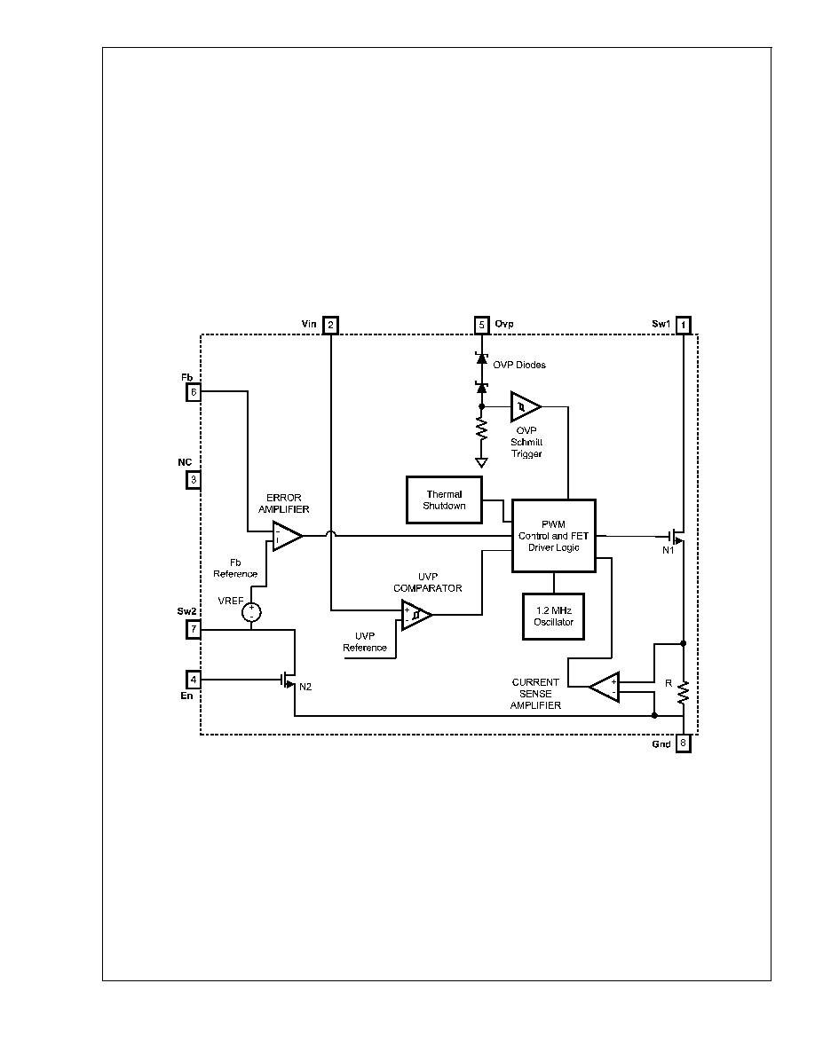
Block Diagram
Operation
The
LM3557
is
a
current-mode
controlled
constant-
frequency step-up converter optimized for the facilitation of
white LED driving/current biasing.
The LM3557's operation can be best understood by the
following device functionality explanation. For the following
device functionality explanation, the block diagram in Figure
2 serves as a functional schematic representation of the
underlying circuit blocks that make up the LM3557. When
the feedback voltage falls below, or rises above, the internal
reference voltage, the error amplifier outputs a signal that is
translated into the correct amount of stored energy within the
inductor that is required to put the feedback voltage back into
regulation when the stored inductor energy is then trans-
ferred to the load. The aforementioned translation is a con-
version of the error amplifier's output signal to the proper
on-time duration of the N1 power field effect transistor (FET).
This conversion allows the inductor's stored energy to in-
crease, or decrease, to a sufficient level that when trans-
ferred to the load will bring the feedback voltage back into
regulation.
20131603
FIGURE 2. Block Diagram
LM3557
www.national.com
4
Operation
(Continued)
An increase in inductor current corresponds to an increase in
the amount of stored energy within the inductor. Conversely,
a decrease in inductor current corresponds to a decrease in
the amount of stored energy. The inductor's stored energy is
released, or transferred, to the load when the N1 power FET
is turned off. The transferred inductor energy replenishes the
output capacitor and keeps the white LED current regulated
at the designated magnitude that is based on the choice of
the R2 resistor. When the N1 power FET is turned on, the
energy stored within the inductor begins to increase while
the output capacitor discharges through the series string of
white LEDs, the R2 resistance, and N2 FET switch to
ground. Therefore, each switching cycle consist of some
amount of energy being stored in the inductor that is then
released, or transferred, to the load to keep the voltage at
the feedback pin in regulation at 510 mV above the Sw2 pin
voltage.
Features:
CYCLE-BY-CYCLE CURRENT LIMIT
The current through the internal power FET (Figure 2: N1) is
monitored to prevent peak inductor currents from damaging
the part. If during a cycle (cycle = 1/switching frequency) the
peak inductor current exceeds the current limit rating for the
LM3557, the internal power FET would be forcibly turned off
for the remaining duration of that cycle.
OVER-VOLTAGE PROTECTION
When the output voltage exceeds the over-voltage protec-
tion (OVP) threshold, the LM3557's internal power FET will
be forcibly turned off until the output voltage falls below the
over-voltage protection threshold minus the 500 mV hyster-
esis of the internal OVP circuitry.
UNDER-VOLTAGE PROTECTION
When the input voltage falls below the under-voltage protec-
tion (UVP) threshold, the LM3557's internal power FET will
be forcibly turned off until the input voltage is above the
designated under-voltage protection threshold plus the
100 mV hysteresis of the internal UVP circuitry.
TRUE SHUTDOWN
When the LM3557 is put into shutdown mode operation
there are no DC current paths to ground. The internal FET
(Figure 2: N2) at the Sw2 pin turns off, leaving the white LED
string open circuited.
THERMAL SHUTDOWN
When the internal semiconductor junction temperature
reaches approximately 150°C, the LM3557's internal power
FET (Figure 2: N1) will be forcibly turned off.
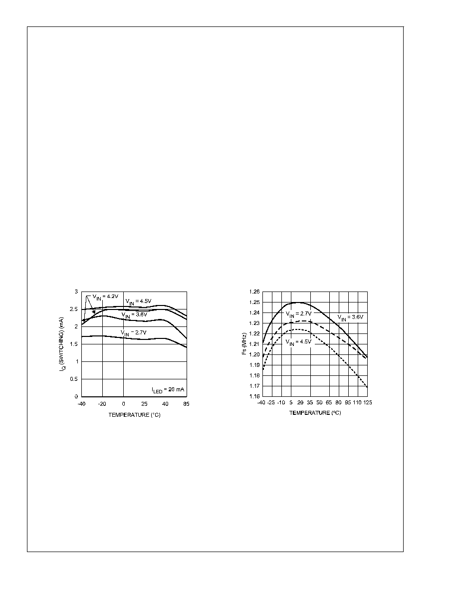
Typical Performance Characteristics
( Circuit in Figure 1: L = DO1608C-223, D = SS16, and LED =
LWT67C. Efficiency:
= P
OUT
/P
IN
= [(V
OUT
V
Fb
) * I
OUT
]/[V
IN
* I
IN
]. T
A
= 25°C, unless otherwise stated).
I
Q
(SWITCHING) vs TEMPERATURE
SWITCHING FREQUENCY vs TEMPERATURE
20131604
20131605
LM3557
www.national.com
5