LM3460-1.2, -1.5
Precision Controller for GTLp and GTL Bus Termination
General Description
The LM3460 is a monolithic integrated circuit designed for
precision control of GTLplus and GTL Bus termination. This
controller is available in a tiny SOT23-5 package, and in-
cludes an internally compensated op amp, a bandgap refer-
ence, an NPN output transistor, and voltage setting resistors.
A trimmed precision bandgap voltage reference utilizes tem-
perature drift curvature correction for excellent voltage stabil-
ity over the operating range. The precision output control en-
ables the termination voltage to maintain tight regulation,
despite fast switching requirements on the bus.
The LM3460 controller is designed to be used with a high
current (
>
7A) NPN pass transistor to provide the high cur-
rent needed for the bus termination. The wide bandwidth of
the feedback loop provides excellent transient response,
and greatly reduces the output capacitance required, thus
reducing cost and board space requirements.
Features
n
Precision output (1%)
n
Output voltage can be adjusted
n
Extremely fast transient response in GTLp and GTL bus
termination
n
Tiny SOT23-5 package
n
Output voltage capability for GTL or GTLp
n
Low temperature coefficient
Applications
n
GTL bus termination (1.2V output 7A)
n
GTLp bus termination (1.5V output 7A)
n
Adjustable high-current linear regulator
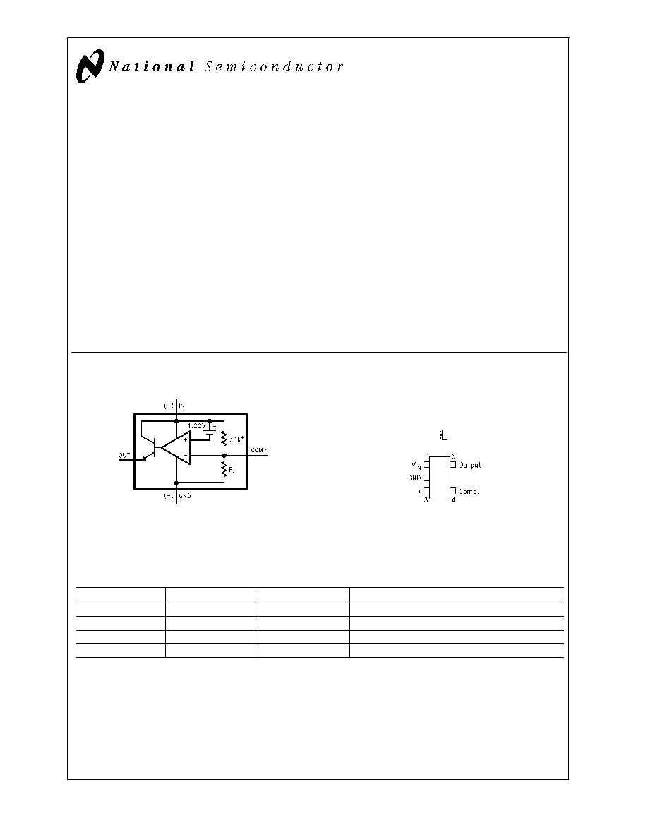
Connection Diagram and Package Information
Ordering Information
Voltage
Order Number
Package Marking
Supplied As
1.5
LM3460M5-1.5
D06A
1000 Unit Increments on Tape and Reel
1.5
LM3460M5X-1.5
D06A
3000 Unit Increments on Tape and Reel
1.2
LM3460M5-1.2
D09A
1000 Unit Increments on Tape and Reel
1.2
LM3460M5X-1.5
D09A
3000 Unit Increments on Tape and Reel
MARKING CODE: The first letter
D
identifies the part as a Driver, and the next two numbers define the voltage for the part. The fourth letter indicates the
grade, with
A
designating the prime grade of product.
AVAILABILITY: The SOT23-5 package is only available in quantity of 1000 on tape and reel (designated by the letters
M5
in the part number), or in quantity
of 3000 on tape and reel (indicated by the letters
M5X
in the part number).
DS012603-1
*
This resistor is not used on the LM3460-1.2.
LM3460 Functional Diagram
5-Lead Outline Package (M5)
Actual Size
DS012603-2
DS012603-3
*
No internal connection, but should be soldered to PC board for best heat
transfer.
Top View
See NS package Number MF05A
July 2000
LM3460-1.2,
-1.5
Precision
Controller
for
GTLp
and
GTL
Bus
T
ermination
� 2000 National Semiconductor Corporation
DS012603
www.national.com
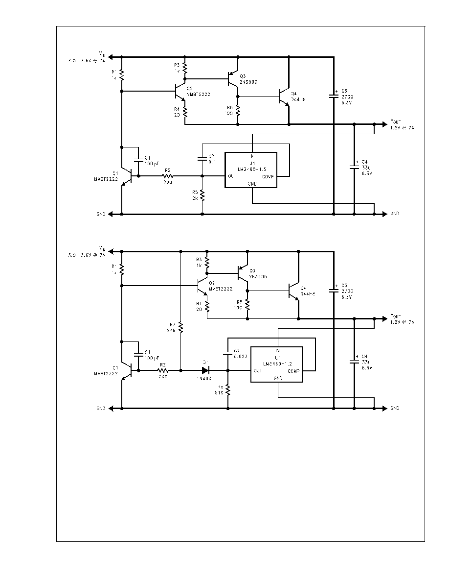
Typical Applications
DS012603-4
FIGURE 1. 1.5V Typical Application (See Application Information Section)
DS012603-5
FIGURE 2. 1.2V Typical Application (See Application Information Section)
LM3460
www.national.com
2

Absolute Maximum Ratings
(Note 1)
If Military/Aerospace specified devices are required,
please contact the National Semiconductor Sales Office/
Distributors for availability and specifications.
Input Voltage V
IN
20V
Output Current
20 mA
Junction Temperature
150�C
Storage Temperature
-65�C to +150�C
Lead Temperature
Vapor Phase (60 sec.)
Infared (15 sec.)
+215�C
+220�C
Power Dissipation (T
A
= 25�C)
(Note 2)
300 mW
ESD Susceptibility (Note 3)
Human Body Model
1500V
See AN-450
Surface Mounting Methods and Their Effect
on Product Reliability
for methods on soldering surface
mount devices.
Operating Ratings
(Note 1)
,
(Note 2)
Ambient Temperature Range
0�C
T
A
+70�C
Output Current
1 mA
Electrical Characteristics
LM3460-1.5
Specifications with standard type face are for T
J
= 25�C, and those with boldface type apply over full Operating Temperature
Range. Unless otherwise specified, (+)IN = V
REG
, V
OUT
= 200 mV
Symbol
Parameter
Conditions
Typ (Note 4)
Limit (Note 5)
Units
V
REG
Regulated Voltage
I
OUT
= 1 mA
1.5
1.515/ 1.530
1.485/1.470
V (max)
V (min)
Regulated Voltage
Tolerance
I
OUT
= 1 mA
�
1 /
�
2
% (max)
I
q
Quiescent Current
I
OUT
= 1 mA
85
125/150
�A (max)
G
m
Transconductance
I
OUT
/
V
REG
20�A
I
OUT
1 mA
V
OUT
= 500 mV
3.3
1/0.5
mA/mV
(min)
V
SAT
Output Saturation
Voltage(Note 6)
V
IN
= V
REG
+ 100 mV
I
OUT
= 1 mA
0.8
0.95
V (max)
I
L
Output Leakage
Current
V
IN
= V
REG
- 100 mV
V
OUT
= 0V
0.1
0.5/1.0
�A (max)
R
F
Internal Feedback
Resistor (See
Functional Diagram)
7.1
8.9
5.3
k
(max)
k
(min)
E
n
Output Noise Voltage
I
OUT
= 1 mA, 10 Hz
f
10kHz
50
�V (rms)
Electrical Characteristics
LM3460-1.2
Specifications with standard type face are for T
J
= 25�C, and those with boldface type apply over full Operating Temperature
Range. Unless otherwise specified, (+)IN = V
REG
, V
OUT
= 200 mV
Symbol
Parameter
Conditions
Typ (Note 4)
Limit (Note 5)
Units
V
REG
Regulated Voltage
I
OUT
= 1 mA
1.220
1.232/ 1.244
1.208/1.196
V (max)
V (min)
Regulated Voltage
Tolerance
I
OUT
= 1 mA
�
1 /
�
2
% (max)
I
q
Quiescent Current
I
OUT
= 1 mA
85
125/150
�A (max)
G
m
Transconductance
I
OUT
/
V
REG
20�A
I
OUT
1 mA
V
OUT
= 200 mV
3.3
1/0.5
mA/mV
(min)
V
SAT
Output Saturation
Voltage(Note 6)
V
IN
= V
REG
+ 100 mV
I
OUT
= 1 mA
0.8
0.95
V (max)
I
L
Output Leakage
Current
V
IN
= V
REG
- 100 mV
V
OUT
= 0V
0.1
0.5/1.0
�A (max)
R
F
Internal Feedback
Resistor (See
Functional Diagram)
10
12.5
7.5
k
(max)
k
(min)
E
n
Output Noise Voltage
I
OUT
= 1 mA, 10 Hz
f
10kHz
50
�V (rms)
LM3460
www.national.com
3

Electrical Characteristics
LM3460-1.2
(Continued)
Note 1: Absolute Maximum Ratings are limits beyond which damage to the device may occur. Operating Ratings indicate conditions for which the device is intended
to be functional, but do not guarantee specific performance limits. For guaranteed specifications and test conditions, see the Electrical Characteristics. The guaran-
teed specifications apply only for the test conditions listed. Some performance characteristics may degrade when the device is not operated under the listed test con-
ditions.
Note 2: The maximum power dissipation must be derated at elevated temperatures and is dictated by T
Jmax
(maximum junction temperature),
JA
(junction ot am-
bient thermal resistance), and T
A
(ambient temperature). The maximum allowable power dissipation at any temperature is (P
Dmax
= (T
Jmax
- T
A
)/
JA
) or the number
given in the Absolute Maximum Ratings, whichever is lower. The typical thermal resistance
JA
when soldered to a printed circuit board is approximately 330� C/W.
Note 3: The human body model is a 100 pF capacitor discharged through a 1.5 k
resistor into each pin.
Note 4: Typical numbers are at 25�C and represent the most likely parametric norm.
Note 5: Limits are 100% production tested at 25�C. Limits over the operating temperature range are guaranteed through correlation using Statistical Quality Control
(SQC) methods. The limits are used to calculate National's Average Outgoing Quality Level (AOQL).
Note 6: V
SAT
= V
REG
- V
OUT
, when the voltage at the IN pin is forced 100mV above the nominal regulating voltage (V
REG
).
LM3460
www.national.com
4
Product Description
The LM3460 is a shunt regulator designed for use as a pre-
cision control element in a feedback loop. The regulated out-
put voltage is sensed between the IN pin and GROUND pin
of the LM3460.
The output of the LM3460 sources current whenever the
voltage at the IN pin reaches the regulated voltage.
This current is used to cut off the drive to the external pass
trnasistor, which provides the negative feedback to force the
output voltage to be the same value as V
REG
.
If the voltage on the IN pin is forced above the V
REG
voltage,
the maximum voltage applied to the IN pin should not ex-
ceed 20V. In addition, an external resistor may be required
on the OUT pin to limit the maximum current to 20 mA.
Compensation
The inverting input of the error amplifier is brought out to sim-
plify closed-loop compensation. Typically, compensation is
provided by a single capacitor connected from the COM-
PENSATION pin to the OUT pin of the LM3460.
Applying a load pulse to the output of the regulator circuit
and observing the output voltage response is a good method
of verifying the stability of the control loop.
If excessive ringing on the output waveform is observed, this
usually indicates marginal stability resulting from insufficient
phase margin.
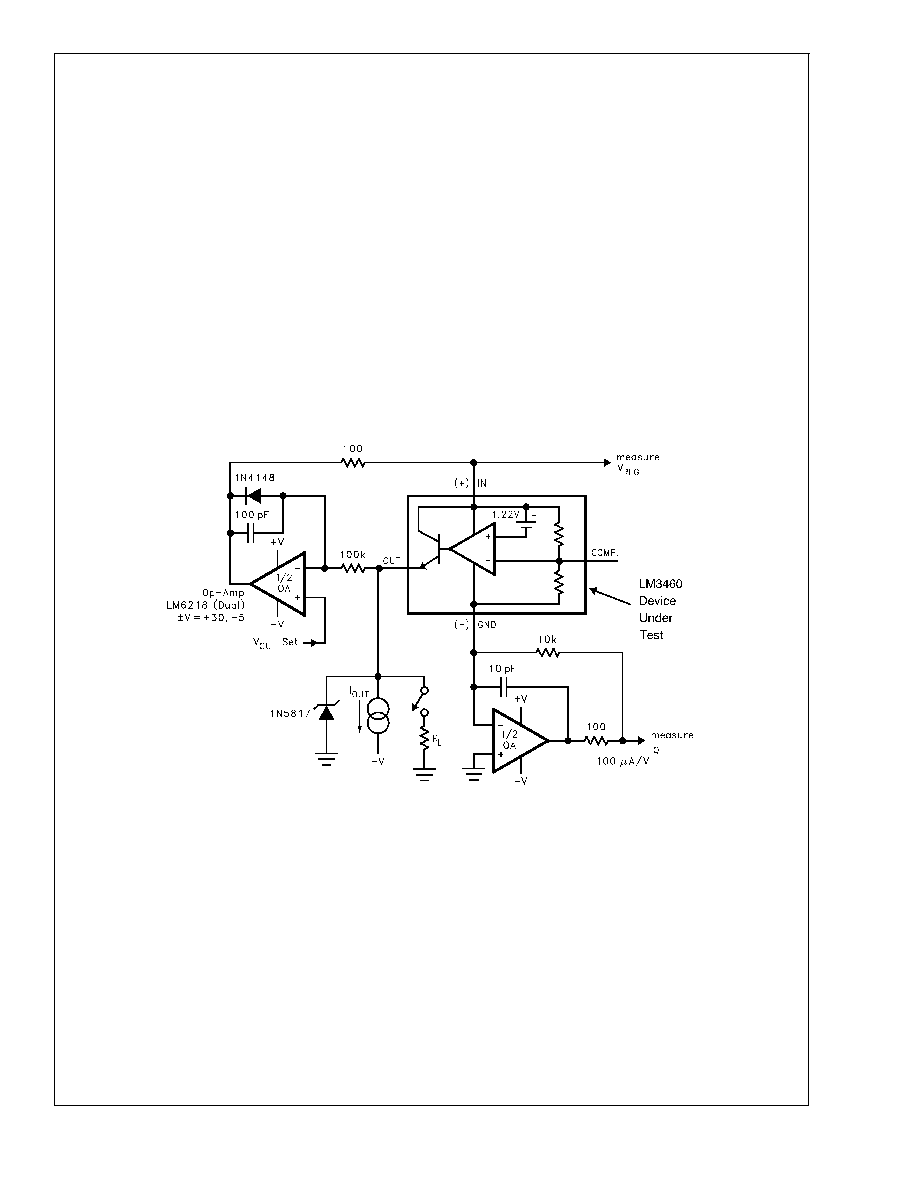
Test Circuit
The test circuit shown in
Figure 3 can be used to measure
various LM3460 parameters. Test conditions are set by forc-
ing the appropriate voltage at the V
OUT
Set test point and se-
lecting the appropriate R
L
or I
OUT
as specified in the Electri-
cal Characteristics section. Use a DVM at the
measure
test
points to read the data.
Setting the Output Voltage
If a regulated voltage is desired which is not available as a
standard voltage, the output voltage may be adjusted by us-
ing an external resistive divider (see
Figure 4):
DS012603-9
V
OUT
Set Note: 0V to 500 mV for LM3460-1.5
0V to 200 mV for LM3460-1.2
FIGURE 3. Test Circuit
LM3460
www.national.com
5