
LM146/LM346
Programmable Quad Operational Amplifiers
General Description
The LM146 series of quad op amps consists of four indepen-
dent, high gain, internally compensated, low power, pro-
grammable amplifiers. Two external resistors (R
SET
) allow
the user to program the gain bandwidth product, slew rate,
supply current, input bias current, input offset current and in-
put noise. For example, the user can trade-off supply current
for bandwidth or optimize noise figure for a given source re-
sistance. In a similar way, other amplifier characteristics can
be tailored to the application. Except for the two program-
ming pins at the end of the package, the LM146 pin-out is
the same as the LM124 and LM148.
Features
(I
SET
=10 ÁA)
n
Programmable electrical characteristics
n
Battery-powered operation
n
Low supply current:
350 ÁA/amplifier
n
Guaranteed gain bandwidth product:
0.8 MHz min
n
Large DC voltage gain:
120 dB
n
Low noise voltage:
28
n
Wide power supply range:
▒
1.5V to
▒
22V
n
Class AB output stage¡no crossover distortion
n
Ideal pin out for Biquad active filters
n
Input bias currents are temperature compensated
Connection Diagram
PROGRAMMING EQUATIONS
Total Supply Current = 1.4 mA (I
SET
/10 ÁA)
Gain Bandwidth Product = 1 MHz (I
SET
/10 ÁA)
Slew Rate = 0.4V/Ás (I
SET
/10 ÁA)
Input Bias Current
50 nA (I
SET
/10 ÁA)
I
SET
= Current into pin 8, pin 9 (see schematic-diagram)
Dual-In-Line Package
DS005654-1
Top View
Order Number LM146J, LM146J/883,
LM346M or LM346N
See NS Package Number
J16A, M16A or N16A
May 1999
LM146/LM346
Programmable
Quad
Operational
Amplifiers
® 1999 National Semiconductor Corporation
DS005654
www.national.com
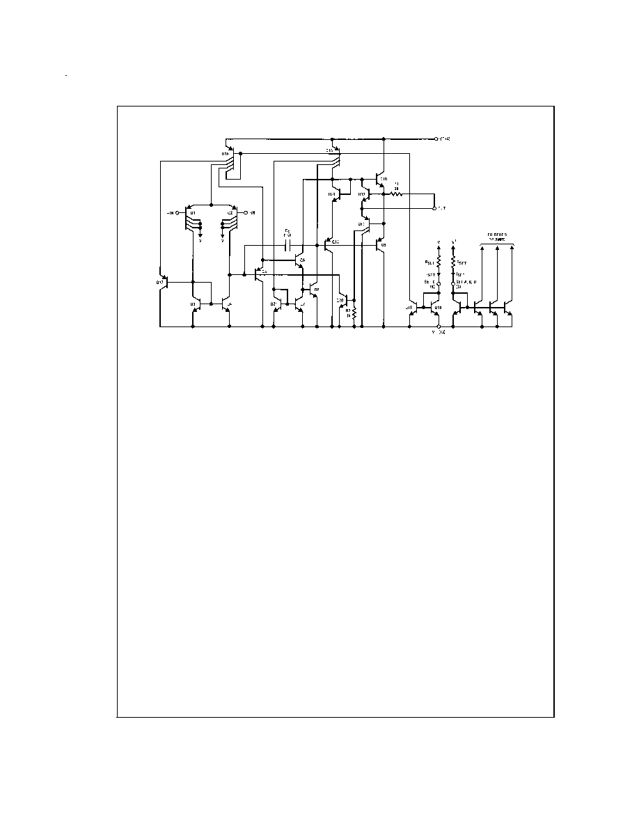
Schematic Diagram
DS005654-2
www.national.com
2
Absolute Maximum Ratings
(Notes 1, 5)
If Military/Aerospace specified devices are required, please contact the National Semiconductor Sales Office/
Distributors for availability and specifications.
LM146
LM346
Supply Voltage
▒
22V
▒
18V
Differential Input Voltage (Note 1)
▒
30V
▒
30V
CM Input Voltage (Note 1)
▒
15V
▒
15V
Power Dissipation (Note 2)
900 mW
500 mW
Output Short-Circuit Duration (Note 3)
Continuous
Continuous
Operating Temperature Range
-55░C to +125░C
0░C to +70░C
Maximum Junction Temperature
150░C
100░C
Storage Temperature Range
-65░C to +150░C
-65░C to +150░C
Lead Temperature (Soldering, 10 seconds)
260░C
260░C
Thermal Resistance (
jA
), (Note 2)
Cavity DIP (J)
Pd
900 mW
900 mW
jA
100░C/W
100░C/W
Small Outline (M)
jA
115░C/W
Molded DIP (N)
Pd
500 mW
jA
90░C/W
Soldering Information
Dual-In-Line Package
Soldering (10 seconds)
+260░C
+260░C
Small Outline Package
Vapor Phase (60 seconds)
+215░C
+215░C
Infrared (15 seconds)
+220░C
+220░C
See AN-450 "Surface Mounting Methods and Their Effect on Product Reliability" for other methods of soldering surface mount de-
vices.
ESD rating is to be determined.
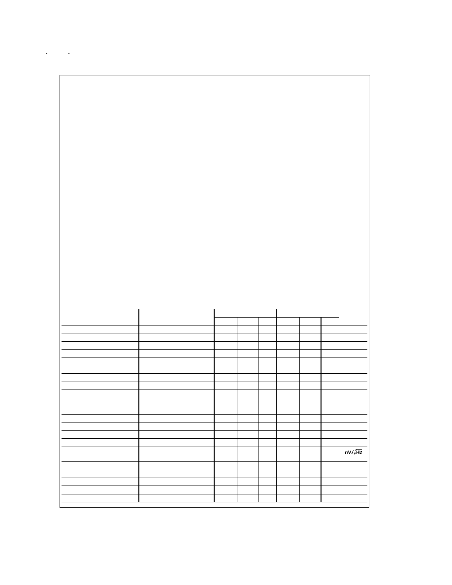
DC Electrical Characteristics
(V
S
=
▒
15V, I
SET
=10 ÁA), (Note 4)
Parameter
Conditions
LM146
LM346
Units
Min
Typ
Max
Min
Typ
Max
Input Offset Voltage
V
CM
=0V, R
S
50
, T
A
=25░C
0.5
5
0.5
6
mV
Input Offset Current
V
CM
=0V, T
A
=25░C
2
20
2
100
nA
Input Bias Current
V
CM
=0V, T
A
=25░C
50
100
50
250
nA
Supply Current (4 Op Amps)
T
A
=25░C
1.4
2.0
1.4
2.5
mA
Large Signal Voltage Gain
R
L
=10 k
,
V
OUT
=
▒
10V,
100
1000
50
1000
V/mV
T
A
=25░C
Input CM Range
T
A
=25░C
▒
13.5
▒
14
▒
13.5
▒
14
V
CM Rejection Ratio
R
S
10 k
, T
A
=25░C
80
100
70
100
dB
Power Supply Rejection Ratio
R
S
10 k
, T
A
=25░C,
80
100
74
100
dB
V
S
=
▒
5 to
▒
15V
Output Voltage Swing
R
L
10 k
, T
A
=25░C
▒
12
▒
14
▒
12
▒
14
V
Short-Circuit
T
A
=25░C
5
20
35
5
20
35
mA
Gain Bandwidth Product
T
A
=25░C
0.8
1.2
0.5
1.2
MHz
Phase Margin
T
A
=25░C
60
60
Deg
Slew Rate
T
A
=25░C
0.4
0.4
V/Ás
Input Noise Voltage
f=1 kHz, T
A
=25░C
28
28
Channel Separation
R
L
=10 k
,
V
OUT
=0V to
120
120
dB
▒
12V, T
A
=25░C
Input Resistance
T
A
=25░C
1.0
1.0
M
Input Capacitance
T
A
=25░C
2.0
2.0
pF
Input Offset Voltage
V
CM
=0V, R
S
50
0.5
6
0.5
7.5
mV
www.national.com
3

DC Electrical Characteristics
(Continued)
(V
S
=
▒
15V, I
SET
=10 ÁA), (Note 4)
Parameter
Conditions
LM146
LM346
Units
Min
Typ
Max
Min
Typ
Max
Input Offset Current
V
CM
=0V
2
25
2
100
nA
Input Bias Current
V
CM
=0V
50
100
50
250
nA
Supply Current (4 Op Amps)
1.7
2.2
1.7
2.5
mA
Large Signal Voltage Gain
R
L
=10 k
,
V
OUT
=
▒
10V
50
1000
25
1000
V/mV
Input CM Range
▒
13.5
▒
14
▒
13.5
▒
14
V
CM Rejection Ratio
R
S
50
70
100
70
100
dB
Power Supply Rejection Ratio
R
S
50
,
76
100
74
100
dB
V
S
=
▒
5V to
▒
15V
Output Voltage Swing
R
L
10 k
▒
12
▒
14
▒
12
▒
14
V
DC Electrical Characteristic
(V
S
=
▒
15V, I
SET
=10 ÁA)
Parameter
Conditions
LM146
LM346
Units
Min
Typ
Max
Min
Typ
Max
Input Offset Voltage
V
CM
=0V, R
S
50
,
0.5
5
0.5
7
mV
T
A
=25░C
Input Bias Current
V
CM
=0V, T
A
=25░C
7.5
20
7.5
100
nA
Supply Current (4 Op Amps)
T
A
=25░C
140
250
140
300
ÁA
Gain Bandwidth Product
T
A
=25░C
80
100
50
100
kHz
DC Electrical Characteristics
(V
S
=
▒
1.5V, I
SET
=10 ÁA)
Parameter
Conditions
LM146
LM346
Units
Min
Typ
Max
Min
Typ
Max
Input Offset Voltage
V
CM
=0V, R
S
50
,
0.5
5
0.5
7
mV
T
A
=25░C
Input CM Range
T
A
=25░C
▒
0.7
▒
0.7
V
CM Rejection Ratio
R
S
50
, T
A
=25░C
80
80
dB
Output Voltage Swing
R
L
10 k
, T
A
=25░C
▒
0.6
▒
0.6
V
Note 1: For supply voltages less than
▒
15V, the absolute maximum input voltage is equal to the supply voltage.
Note 2: The maximum power dissipation for these devices must be derated at elevated temperatures and is dictated by T
jMAX
,
jA
, and the ambient temperature,
T
A
. The maximum available power dissipation at any temperature is P
d
=(T
jMAX
- T
A
)/
jA
or the 25░C P
dMAX
, whichever is less.
Note 3: Any of the amplifier outputs can be shorted to ground indefinitely; however, more than one should not be simultaneously shorted as the maximum junction
temperature will be exceeded.
Note 4: These specifications apply over the absolute maximum operating temperature range unless otherwise noted.
Note 5: Refer to RETS146X for LM146J military specifications.
www.national.com
4
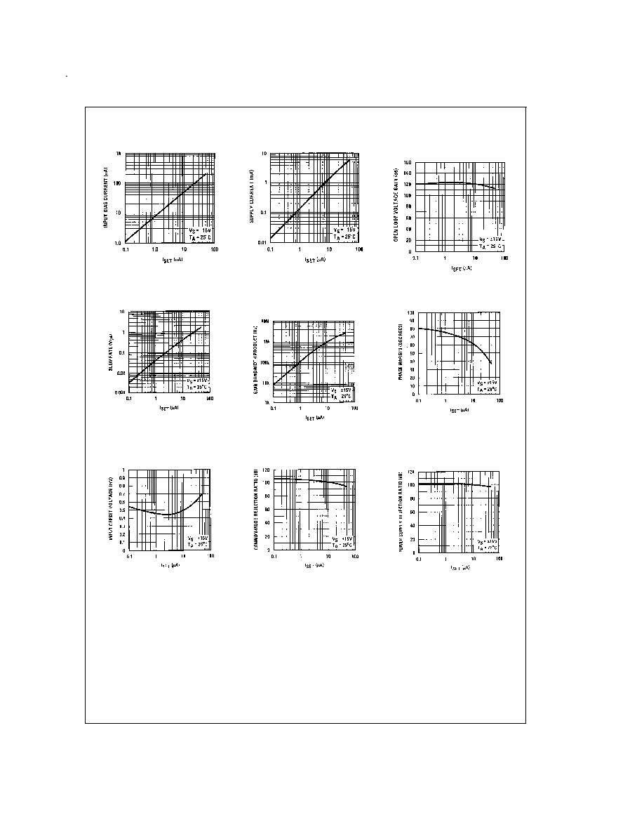
Typical Performance Characteristics
Input Bias Current vs I
SET
DS005654-44
Supply Current vs I
SET
DS005654-45
Open Loop Voltage Gain
vs I
SET
DS005654-46
Slew Rate vs I
SET
DS005654-47
Gain Bandwidth Product
vs I
SET
DS005654-48
Phase Margin vs I
SET
DS005654-49
Input Offset Voltage
vs I
SET
DS005654-50
Common-Mode Rejection
Ratio vs I
SET
DS005654-51
Power Supply Rejection
Ratio vs I
SET
DS005654-52
www.national.com
5