LM2403
Monolithic Triple 4.5 nS CRT Driver
General Description
The LM2403 is an integrated high voltage CRT driver circuit
designed for use in high resolution color monitor applica-
tions. The IC contains three high input impedance, wide
band amplifiers which directly drive the RGB cathodes of a
CRT. Each channel has its gain internally set to -14 and can
drive CRT capacitive loads as well as resistive loads pre-
sented by other applications, limited only by the package's
power dissipation.
The IC is packaged in an industry standard 11 lead TO-220
molded plastic power package. See thermal considerations
on page 5.
Features
n
Rise/fall times typically 4.5 nS with 8 pF load at 40 V
pp
n
Well matched with LM1283 video preamp
n
Output swing capability: 60 V
pp
for V
CC
= 80V
n
1V to 5V input range
n
Stable with 0 pFş20 pF capacitive loads and inductive
peaking networks
n
Convenient TO-220 staggered lead package style
n
Standard LM240X Family Pinout which is designed for
easy PCB layout
Applications
n
CRT driver for color monitors with display resolutions up
to 1600 x 1200
n
Pixel clock frequency up to 160 MHz
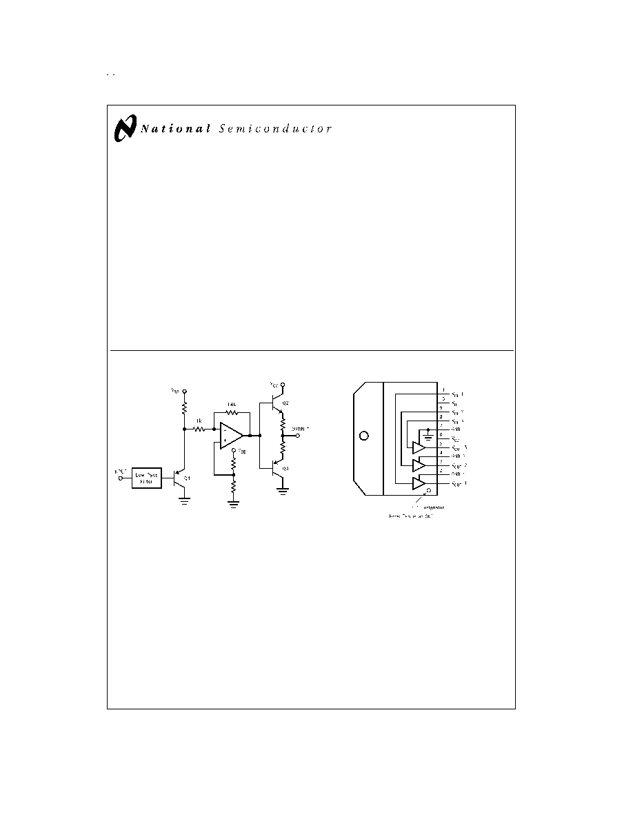
Schematic and Connection Diagrams
DS100082-1
DS100082-2
Top View
Order Number LM2403T
FIGURE 1. Simplified Schematic Diagram (One Channel)
August 1999
LM2403
Monolithic
T
riple
4.5
nS
CRT
Driver
ę 1999 National Semiconductor Corporation
DS100082
www.national.com

Absolute Maximum Ratings
(Notes 1, 2)
If Military/Aerospace specified devices are required,
please contact the National Semiconductor Sales Office/
Distributors for availability and specifications.
Supply Voltage (V
CC
)
+90V
Bias Voltage (V
BB
)
+16V
Input Voltage (V
IN
)
-0.5V to V
BIAS
+0.5V
Storage Temperature Range (T
STG
)
-65░C to +150░C
Lead Temperature
(Soldering,
<
10 sec.)
300░C
ESD Tolerance, Human Body Model
2 kV
Machine Model
250V
Operating Range
(Note 3)
V
CC
+60V to +85V
V
BB
+8V to +15V
V
IN
+1V to +5V
V
OUT
+10V to +70V
Case Temperature
-20░C to +100░C
Do not operate the part without a heat sink.
Note 1: Absolute Maximum Ratings indicate limits beyond which damage to
the device may occur.
Note 2: All voltages are measured with respect to GND, unless otherwise
specified.
Note 3: Operating ratings indicate conditions for which the device is func-
tional, but do not guarantee specific performance limits. For guaranteed
specifications and test conditions, see the Electrical Characteristics. The
guaranteed specifications apply only for the test conditions listed. Some per-
formance characteristics may change when the device is not operated under
the listed test conditions.
Electrical Characteristics
(See
Figure 2 for Test Circuit)
Unless otherwise noted: V
CC
= +80V, V
BB
= +12 V, V
IN
= +3.3 V
DC
, C
L
= 8 pF, L
P
= 0.22 ÁH, Output = 40 V
PP
at 1 MHz, T
A
=
25░C.
Symbol
Parameter
Condition
LM2403
Units
Min
Typical
Max
I
CC
Supply Current
Per Channel, No Output Load
26
mA
I
BB
Bias Current
All Three Channels
11.5
mA
V
OUT
DC Output Voltage
No AC Input Signal, V
IN
= 2.8 V
48
52
56
V
DC
A
V
DC Voltage Gain
No AC Input Signal
-12
-14
-16
A
V
Gain Matching
(Note 4), No AC Input Signal
1.0
dB
LE
Linearity Error
(Notes 4, 5), No AC Input Signal
3.5
%
t
R
Rise Time
10% to 90%
4.5
nS
t
F
Fall Time
90% to 10%
4.5
nS
OS
Overshoot
3
%
Note 4: Calculated value from Voltage Gain test on each channel.
Note 5: Linearity Error is the variation in dc gain from V
IN
= 1.5V to V
IN
= 5V.
Note 6: Input from signal generator: t
r
, t
f
<
1 nS.
AC Test Circuit
Figure 2 shows a typical test circuit for evaluation of the LM2403. This circuit is designed to allow testing of the LM2403 in a 50
environment without the use of an expensive FET probe. The 4950
resistor at the output forms a 100:1 voltage divider when
connected to a 50
load.
DS100082-3
FIGURE 2. Test Circuit (One Channel)
www.national.com
2

AC Test Circuit
(Continued)
DS100082-4
FIGURE 3. V
OUT
vs V
IN
DS100082-5
FIGURE 4. Speed vs Temp.
DS100082-6
FIGURE 5. Pulse Response
DS100082-7
FIGURE 6. Power Dissipation vs Frequency
DS100082-8
FIGURE 7. Speed vs Offset
DS100082-9
FIGURE 8. Pulse Response with V
CC
= 70 V
DC
www.national.com
3

Theory of Operation
The LM2403 is a high voltage monolithic three channel CRT
driver suitable for high resolution display applications. The
LM2403 operates using 80V and 12V power supplies. The
part is housed in the industry standard 11-lead TO-220
molded plastic power package.
The simplified circuit diagram of the LM2403 is shown in
Fig-
ure 1. A PNP emitter follower, Q1, provides input buffering.
The 14 k
feedback resistor and the 1 k
input resistor sets
the gain of the inverting op-amp to -14. Emitter followers Q2
and Q3 isolate the output of the feedback amplifier from the
capacitance of the CRT cathode, and make the circuit rela-
tively insensitive to load capacitance.
Figure 2 shows a typical test circuit for evaluation of the
LM2403. This circuit is designed to allow testing of the
LM2403 in a 50
environment without the use of an expen-
sive FET probe. In this test circuit, two low inductance resis-
tors in series totaling 4.95 k
form a 100:1 wideband low ca-
pacitance probe when connected to a 50
cable and load.
The input signal from the generator is ac coupled to the base
of Q1.
Figure 9 shows the large signal sine wave frequency re-
sponse of the LM2403. The frequency response rolls off very
rapidly above the bandwidth limit of the amplifier. There are
two reasons for this fast response roll-off:
1.
The LM2403 contains an input low pass filter to help re-
move unwanted high frequency harmonics that can
cause EMI problems. This filter does not significantly af-
fect the rise and fall times of the signal as it operates
above the -3 dB bandwidth of the device.
2.
The internal feedback network of the closed loop ampli-
fier holds the gain at -14 until the loop gain drops below
unity. Above this frequency, the amplifier response falls
with the open loop gain of the amplifier, as the feedback
ceases to have any significant effect. There is also a
change in the impedance match between the op-amp
and the emitter follower output stage with large signals
at higher frequencies. This creates a gain boost that ex-
tends the bandwidth, then gives a sudden roll off as
shown in
Figure 9. The exact response of this roll off
may vary slightly depending upon operating conditions,
signal amplitude etc.
In both cases, the fast roll of the high frequency harmonics
will help to limit the creation of high frequency EMI harmon-
ics, without limiting video rise and fall time characteristics.
However, due to the very fast switching speeds of the de-
vice, good layout design for EMI is CRITICAL. Path lengths
and loop areas of the video signals must be kept to a mini-
mum.
Application Hints
INTRODUCTION
National Semiconductor (NSC) is committed to providing ap-
plication information that assists our customers in obtaining
the best performance possible from our products. The follow-
ing information is provided in order to support this commit-
ment. The reader should be aware that the optimization of
performance was done using a specific printed circuit board
designed at NSC. Variations in performance can be realized
due to physical changes in the printed circuit board and the
application. Therefore, the designer should know that com-
ponent value changes may be required in order to optimize
performance in a given application. The values shown in this
document can be used as a starting point for evaluation pur-
poses. When working with high bandwidth circuits, good lay-
out practices are also critical to achieving maximum perfor-
mance.
POWER SUPPLY BYPASS
Since the LM2403 is a high bandwidth amplifier, proper
power supply bypassing is critical for optimum performance.
Improper power supply bypassing can result in large over-
shoot, ringing and oscillation. A 0.1 ÁF capacitor should be
connected from the supply pin, Vcc, to ground, as close to
the supply and ground pins as is practical. Additionally, a
10 ÁF to 100 ÁF electrolytic capacitor should be connected
from the supply pin to ground. The electrolytic capacitor
should also be placed reasonably close to the LM2403's
supply and ground pins. A 0.1ÁF capacitor should be con-
nected from the bias pin, Vbb, to ground, as close as is prac-
tical to the part.
ARC PROTECTION
During normal CRT operation, internal arcing may occasion-
ally occur. Spark gaps, in the range of 200V, connected from
the CRT cathodes to CRT ground will limit the maximum volt-
age, but to a value that is much higher than allowable on the
LM2403. This fast, high voltage, high energy pulse can dam-
age the LM2403 output stage. The application circuit shown
in
Figure 10 is designed to help clamp the voltage at the out-
put of the LM2403 to a safe level. The clamp diodes should
have a fast transient response, high peak current rating, low
series impedance and low shunt capacitance. FDH400 or
equivalent diodes are recommended. D1 and D2 should
have short, low impedance connections to V
CC
and ground
respectively. The cathode of D1 should be located very close
to a separately decoupled bypass capacitor. The ground
connection of the diode and the decoupling capacitor should
be very close to the LM2403 ground. This will significantly re-
duce the high frequency voltage transients that the LM2403
would be subjected to during an arcover condition. Resistor
R2 limits the arcover current that is seen by the diodes while
R1 limits the current into the LM2403 as well as the voltage
stress at the outputs of the device. R2 should be a 1/2W
solid carbon type resistor. R1 can be a 1/4W metal or carbon
film type resistor. Inductor L1 is critical to reduce the initial
high frequency voltage levels that the LM2403 would be sub-
jected to. Having large value resistors for R1 and R2 would
be desirable, but this has the effect of increasing rise and fall
times. The inductor will not only help protect the device but it
DS100082-16
FIGURE 9.
www.national.com
4

Application Hints
(Continued)
will also help optimize rise and fall times as well as minimize
EMI. For proper arc protection, it is important to not omit any
of the arc protection components shown in
Figure 10.
OPTIMIZING TRANSIENT RESPONSE
Referring to
Figure 10, there are three components (R1, R2
and L1) that can be adjusted to optimize the transient re-
sponse of the application circuit. Increasing the values of R1
and R2 will slow the circuit down while decreasing over-
shoot. Increasing the value of L1 will speed up the circuit as
well as increase overshoot. It is very important to use induc-
tors with very high self-resonant frequencies, preferably
above 300 MHz. Ferrite core inductors from J.W. Miller Mag-
netics (part # 78FR12M) were used for optimizing the perfor-
mance of the device in the NSC application board. The val-
ues shown in
Figure 10 can be used as a good starting point
for the evaluation of the LM2403. The NSC demo board also
has a position open to add a resistor in parallel with L1. This
resistor can be used to help control overshoot. Using vari-
able resistors for R1 and the parallel resistor is a great way
to help dial in the values needed for optimum performance in
a given application.
Pull-up Resistors
Optimizing the performance of the LM2403 does require the
use of pull-up resistors at the outputs of the CRT driver.
These resistors are shown as R100, R101, and R102 in the
schematic. If you have a demo board form National please
note that these resistors have been added on the back of the
board since there is no PCB location for the pull-up resistors.
Because of the improved performance with these resistors,
all demo boards have been shipped with the added pull-up
resistors. The LM2403 does have some crossover distortion,
normal for any AB amplifier such as the LM2403. Adding the
pull-up resistors does add more bias to Q3 (
Figure 1) thus
minimizing the crossover distortion. The LM2403 is normally
used in high end monitors, so it is highly recommended that
the 12k pull-up resistors be used in any design using the
LM2403. Selecting a 12k resistor provides the needed
pull-up current and limits the worst case power dissipation to
1/4W (white level at 25V).
In some applications pull-down resistors may be preferred.
Using 12k resistors gives acceptable performance, but this
will require the use of 1/2W resistors. Normally the power
save mode establishes whether pull-up or pull-down resis-
tors are preferred. If the setup of the power save mode in the
monitor gives a low output at the LM2403, then the pull-down
resistors would be preferred, if the 80V supply is still turned
on.
Effect of Load Capacitance
The output rise and fall times as well as overshoot will vary
as the load capacitance varies. The values of the output cir-
cuit (R1, R2 and L1 in
Figure 10) should be chosen based on
the nominal load capacitance. Once this is done the perfor-
mance of the design can be checked by varying the load
based on what the expected variation will be.
For example, suppose you needed to drive a 10 pF (
▒
20%)
load with a 40V
p-p
waveform. First, you would pick the values
of R1, R2 and L1 that give the desired response with a 10 pF
load. Then you would test the design when driving an 8 pF
load and a 12 pF load. The table below summarizes the re-
sults from doing this exercise in a test board in the NSC lab.
The output signal swing was 40V
p-p
from 65V to 25V.
Parameter
8 pF
10 pF
12 pF
Rise Time
4.1
4.2
4.3
Overshoot
1%
5%
10%
Fall Time
4.4
4.6
4.7
Overshoot
1%
2%
5%
The example above clearly demonstrates the importance of
having a good estimate of the range of the load capacitance.
Effect of Offset
Figure 7 shows the variation in rise and fall times when the
output offset of the device is varied from 30 V
DC
to 50 V
DC
.
The rise time shows about twice as much variation as the fall
time, however the maximum variation relative to the center
data point (40 V
DC
) is less than 10%.
Operation with V
CC
= 70V
The closed loop topography of the LM2403 allows operation
down to 10V above ground. If the user can limit the white
level between 10V and 20V, then operation with V
CC
= 70V
is possible. Operating the LM2403 with V
CC
= 70V will re-
quire the same current even though the supply voltage has
dropped by 12.5%. This results in a power savings of 12.5%
(as high a 1.5W), allowing a reduction in the size of the heat-
sink.
Figure 8 shows the output waveform of the LM2403 op-
erating at a white level of 15V, and a peak-to-peak output
swing of 40V. Below is a summary of the LM2403 rise and
fall times with various output offset levels with V
CC
= 70V.
DS100082-10
FIGURE 10. One Channel of the LM2403 with the Recommended Arc Protection Circuit
www.national.com
5