
TL H 11884
LM1208LM1209
130
MHz100
MHz
RGB
Video
Amplifier
System
with
Blanking
January 1996
LM1208 LM1209
130 MHz 100 MHz RGB Video Amplifier System
with Blanking
General Description
The LM1208 LM1209 is a very high frequency video amplifi-
er system intended for use in high resolution RGB monitor
applications In addition to the three matched video amplifi-
ers the LM1208 LM1209 contains three gated single end-
ed input black level clamp comparators for brightness con-
trol three matched DC controlled attenuators for contrast
control and three DC controlled drive attenuators providing
independent full range gain control in each channel for wide
range white balance All DC control inputs offer high input
impedance and an operation range from 0V to 4V for easy
interface
to
bus
controlled
alignment
systems
The
LM1208 LM1209 also contains a blanking circuit which
clamps the video output voltage during blanking to within
0 1V above ground This feature provides blanking capabili-
ty at the cathodes of the CRT A spot killer is provided for
CRT phosphor protection during power-down
Features
Y
Three wideband video amplifiers 130 MHz
b
3 dB
(4 V
PP
output)
Y
Matched (
g
0 1 dB or 1 2%) attenuators for contrast
control
Y
Three externally gated single ended input comparators
for cutoff and brightness control
Y
0V to 4V high input impedance DC contrast control
(
l
40 dB range)
Y
0V to 4V high input impedance DC full range gain con-
trol (Drive) for each video channel (
l
40 dB range)
Y
Spot killer blanks outputs when V
CC
k
10 6V
Y
Capable of 7 V
PP
output swing (slight reduction in
bandwidth)
Y
Output stage blanking
Y
Output stage directly drives most hybrid or discrete
CRT drivers
Applications
Y
High resolution RGB CRT monitors
Y
Video AGC amplifiers
Y
Wideband amplifiers with gain and DC offset controls
Y
Interface amplifiers for LCD or CCD systems
Block and Connection Diagram
TL H 11884 Ł 1
FIGURE 1
Order Number LM1208N or LM1209N
See NS Package Number N28B
C1996 National Semiconductor Corporation
RRD-B30M66 Printed in U S A

Absolute Maximum Ratings
(Note 1)
If Military Aerospace specified devices are required
please contact the National Semiconductor Sales
Office Distributors for availability and specifications
Supply Voltage (V
CC
)
Pins 3 11 22 23 25 (Note 3)
15V
Peak Video Output Source Current
(Any One Amp) Pins 17 20 or 26
28 mA
Voltage at Any Input Pin (V
IN
)
V
CC
t
V
IN
t
GND
Power Dissipation (P
D
)
(Above 25 C Derate Based on i
JA
and T
J
)
2 5W
Thermal Resistance (i
JA
)
50 C W
Junction Temperature (T
J
)
150 C
ESD Susceptibility (Note 4)
2 kV
Pins 12 13 and 14
1 9 kV
Storage Temperature
b
65 C to 150 C
Lead Temperature (Soldering 10 sec )
265 C
Operating Ratings
(Note 2)
Temperature Range
b
20 C to 80 C
Supply Voltage (V
CC
)
10 8V
s
V
CC
s
13 2V
DC Electrical Characteristics
See DC Test Circuit
(Figure 2 ) T
A
e
25 C V
CC1
e
V
CC2
e
12V V
12
e
4V
V
14
e
0V V
cut-off
e
1 0V V
13
e
4V V
drive
e
4V unless otherwise stated
Symbol
Parameter
Conditions
Typical
Limit
Units
(Note 5)
(Note 6)
I
S
Supply Current
V
CC1
a
V
CC2
R
L
e
%
(Note 7)
90
105
mA (max)
V
4 6 9
Video Amplifier Input Bias Voltage
2 8
V
R
IN
Video Input Resistance
Any One Amplifier
20
kX
V
14l
Clamp Gate Low Input Voltage
Clamp Comparators On
1 2
0 8
V (max)
V
14h
Clamp Gate High Input Voltage
Clamp Comparators Off
1 6
2 0
V (min)
I
14l
Clamp Gate Low Input Current
V
14
e
0V
b
1
b
5
m
A (max)
I
14h
Clamp Gate High Input Current
V
14
e
12V
0 01
1 0
m
A (max)
I
clamp
Clamp Cap Charge Current
Clamp Comparators On
g
750
g
500
m
A (min)
I
bias
Clamp Cap Bias Discharge Current
Clamp Comparators Off
500
nA
V
13l
Blank Gate Low Input Voltage
Blank Gate On
1 2
0 8
V (max)
V
13h
Blank Gate High Input Voltage
Blank Gate Off
1 6
2 0
V (min)
I
13l
Blank Gate Low Input Current
V
13
e
0V
b
8 5
b
11 0
m
A (max)
I
13h
Blank Gate High Input Current
V
13
e
12V
0 01
1 0
m
A (max)
V
OL
Video Output Low Voltage
V
cut-off
e
0V
0 15
0 5
V (max)
V
OH
Video Output High Voltage
V
cut-off
e
9V
7 5
7
V (min)
V
O(1V)
Video Black Level Output Voltage
V
cut-off
e
1V
1 0
V (Note 8)
D
V
O(1V)
Video D Black Level Output Voltage
Between Any Two Amplifiers
g
100
mV (max)
V
cut-off
e
1V
V
OL
(blanked)
Video Output Blanked Voltage
V
13
e
0V
35
70
mV (max)
I
12 15 18 or 28
Contrast Drive Control Input Current
V
contrast
e
V
drive
e
0V to 4V
b
250
nA
I
16 19 and 27
Cut-Off Control Input Current (All Inputs)
V
cut-off
e
0V to 4V
b
500
nA
V
SPOT
Spot Killer Voltage
V
CC
Adjusted to Activate
10 4
10 8
V (max)
http
www national com
2

AC Electrical Characteristics
See AC Test Circuit
(Figure 3) T
A
e
25 C V
CC1
e
V
CC2
e
12V Manually
adjust Video Output pins 17 20 and 26 to 4V DC for the AC test unless otherwise stated (Note 14)
Symbol
Parameter
Conditions
Typical
Limit
Units
(Note 5)
(Note 6)
A
V max
Video Amplifier Gain
V12
e
4V V
IN
e
635 mV
PP
7 0
6 0
V V (min)
V
drive
e
4V
16 9
15 6
dB (min)
D
A
V 2V
Contrast Attenuation
2V
Ref A
V
max V12
e
2V
b
6
dB
D
A
V 0 25V
Contrast Attenuation
0 25V
Ref A
V
max V12
e
0 25V
b
40
dB
D
Drive
2V
Drive Attenuation
2V
Ref A
V
max V
drive
e
2V
b
6
dB
D
Drive
0 25V
Drive Attenuation
0 25V
Ref A
V
max V
drive
e
0 25V
b
40
dB
A
V match
Absolute Gain Match
A
V
max
V12
e
4V V
drive
e
4V (Note 9)
g
0 3
dB
A
V track1
Gain Change Between Amplifiers
V12
e
4V to 2V (Notes 9 10)
g
0 1
dB
THD
Video Amplifier Distortion
V
O
e
1 V
PP
f
e
10 kHz
1
%
f (
b
3 dB)
Video Amplifier Bandwidth
V12
e
4V V
drive
e
4V
LM1208
130
MHz
(Notes 11 12)
V
O
e
4 V
PP
LM1209
100
t
r
(Video)
Video Output Rise Time (Note 11)
V
O
e
4 V
PP
LM1208
2 8
ns
LM1209
3 2
t
f
(Video)
Video Output Fall Time (Note 11)
V
O
e
4 V
PP
LM1208
3 4
ns
LM1209
3 6
V
sep
10 kHz
Video Amplifier 10 kHz Isolation
V12
e
4V (Note 13)
b
70
dB
V
sep
10 MHz
Video Amplifier 10 MHz Isolation
V12
e
4V (Notes 11 13)
b
50
dB
t
r
(Blank)
Blank Output Rise Time (Note 11)
Blank Output
e
1 V
PP
7
ns
t
f
(Blank)
Blank Output Fall Time (Note 11)
Blank Output
e
1 V
PP
7
ns
t
pw
(Clamp)
Min Back Porch Clamp Pulse Width
200
ns
Note 1
Absolute Maximum Ratings indicate limits beyond which damage to the device may occur
Note 2
Operating Ratings indicate conditions for which the device is functional but do not guarantee specific performance limits For guaranteed specifications
and test conditions see the Electrical Characteristics The guaranteed specifications apply only for the test conditions listed Some performance characteristics
may degrade when the device is not operated under the listed test conditions
Note 3
V
CC
supply pins 3 11 22 23 25 must be externally wired together to prevent internal damage during V
CC
power on off cycles
Note 4
Human body model 100 pF discharged through a 1 5 kX resistor
Note 5
Typical specifications are specified at
a
25 C and represent the most likely parametric norm
Note 6
Tested limits are guaranteed to National's AOQL (Average Outgoing Quality Level)
Note 7
The supply current specified is the quiescent current for V
CC1
and V
CC2
with R
L
e
%
see
Figure 2's test circuit The supply current for V
CC2
(pin 23) also
depends on the output load With video output at 1V DC the additional current through V
CC2
is 8 mA for
Figure 2's test circuit
Note 8
Output voltage is dependent on load resistor Test circuit uses R
L
e
390X
Note 9
Measure gain difference between any two amplifiers V
IN
e
635 mV
PP
Note 10 D
A
V
track is a measure of the ability of any two amplifiers to track each other and quantifies the matching of the three attenuators It is the difference in
gain change between any two amplifiers with the contrast voltage (V12) at either 4V or 2V measured relative to an A
V
max condition V12
e
4V For example at A
V
max the three amplifiers' gains might be 17 1 dB 16 9 dB and 16 8 dB and change to 11 2 dB 10 9 dB and 10 7 dB respectively for V12
e
2V This yields the
measured typical
g
0 1 dB channel tracking
Note 11
When measuring video amplifier bandwidth or pulse rise and fall times a double sided full ground plane printed circuit board without socket is
recommended Video amplifier 10 MHz isolation test also requires this printed circuit board The reason for a double sided full ground plane PCB is that large
measurement variations occur in single sided PCBs
Note 12
Adjust input frequency from 10 MHz (A
V
max reference level) to the
b
3 dB corner frequency (f
b
3 dB
)
Note 13
Measure output levels of the other two undriven amplifiers relative to the driven amplifier to determine channel separation Terminate the undriven
amplifier inputs to simulate generator loading Repeat test at f
IN
e
10 MHz for V
sep 10 MHz
Note 14
During the AC tests the 4V DC level is the center voltage of the AC output signal For example if the output is 4 V
PP
the signal will swing between 2V DC
and 6V DC
http
www national com
3
Typical Performance Characteristics
(V
CC
e
12V T
A
e
25 C unless otherwise specified)
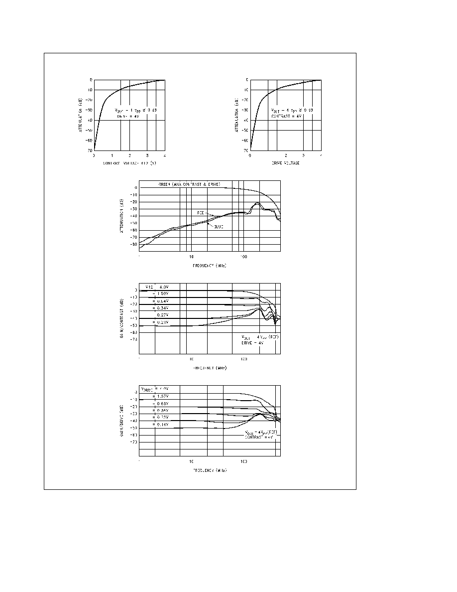
Attenuation vs Contrast Voltage
TL H 11884 Ł 3
Attenuation vs Drive Voltage
TL H 11884 Ł 2
LM1208 Crosstalk vs Frequency
TL H 11884 Ł 4
LM1208 Contrast vs Frequency
TL H 11884 Ł 5
LM1208 Drive vs Frequency
TL H 11884 Ł 6
http
www national com
4
Typical Performance Characteristics
(V
CC
e
12V T
A
e
25 C unless otherwise specified) (Continued)
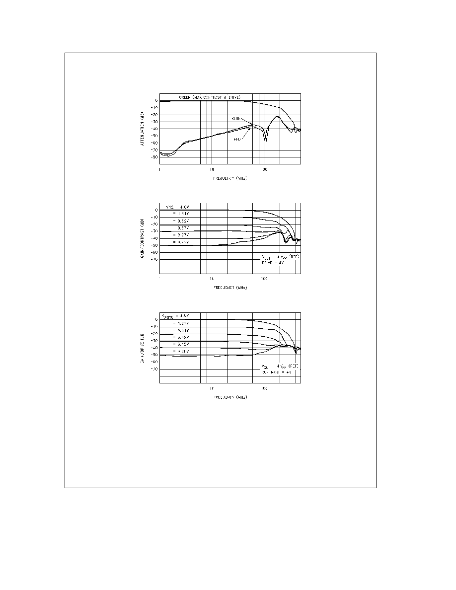
LM1209 Crosstalk vs Frequency
TL H 11884 Ł 25
LM1209 Contrast vs Frequency
TL H 11884 Ł 26
LM1209 Drive vs Frequency
TL H 11884 Ł 27
http
www national com
5