TL F 12437
DP83957
10
Mbs
Repeater
Information
Base
PRELIMINARY
June 1995
DP83957 10 Mb s Repeater Information Base
General Description
The DP83957 Repeater Information Base ``RIB'' allows ef-
fective implementation of managed multi-port 10 Mb s
ethernet repeater hubs The device supports all the neces-
sary Port Attributes for the IEEE 802 3k standard (Layer
Management for 10 Mb s Baseband Repeaters) This de-
vice is designed to be interfaced with Repeater Interface
Controllers (DP83950 2) and gathers attributes on a per-
port per-packet basis
The DP83957 collects management attributes via the
DP83950 2 Management Bus and stores this information in
an external SRAM The DP83957 can be programmed to
collect information for up to two DP83950 2 on a shared
Management Bus It can also be used in a dedicated one
DP83957 per DP83950 2 architecture The attributes stored
in external SRAM can be easily accessed through the
DP83957 by an 8-bit multiplexed Address Data bus
Features
Y
Fully IEEE 802 3K-July 1992 compatible
Y
Supports up to two DP83950 2
Y
Supports generic 1k x 8 or 2k x 8 SRAMs with variable
access times of up to 45 ns
Y
Guarantees at least one attribute access by the micro-
processor in the busiest network scenario
Y
Pipelined architecture for processing back to back
frames
Y
Supports maskable interrupts for status and error re-
porting on a shared interrupt pin
Y
Detection and notification of DP83950 Management
Bus errors
Y
Detection and notification of overflow of attribute coun-
ters
Y
80-pin PQFP package
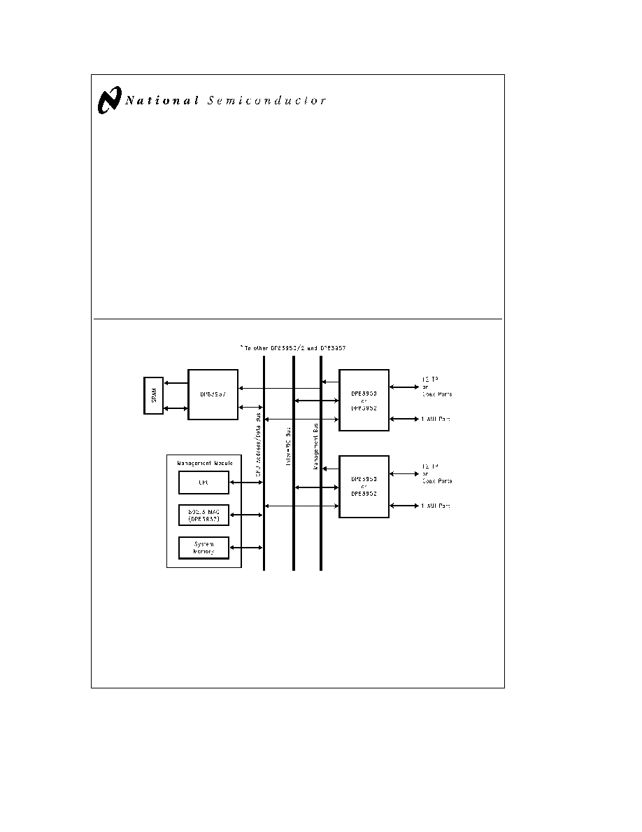
1 0 System Diagram
TL F 12437 � 1
TRI-STATE
is a registered trademark of National Semiconductor Corporation
C1995 National Semiconductor Corporation
RRD-B30M105 Printed in U S A

Table of Contents
1 0 SYSTEM DIAGRAM
2 0 PIN CONNECTION DIAGRAM
3 0 PIN DESCRIPTION
3 1 CPU Interface
3 2 SRAM Interface
3 3 Management Bus Interface
3 4 Miscellaneous Pins
3 5 Pin Type Designation
4 0 BLOCK DIAGRAM
5 0 FUNCTIONAL DESCRIPTION
5 1 SRAM Interface
5 1 1 SRAM Configuration
5 1 2 SRAM Read Operation
5 1 3 SRAM Write Operation
5 1 4 SRAM Memory Map
5 1 5 SRAM Address Format
5 2 Management Interface
5 2 1 Management Configuration
5 2 2 Management Bus Interface
5 2 3 Management Bus Processing
5 2 4 Port Attributes
5 2 5 Port Attribute Status
5 2 6 Port Attribute Overflow
5 3 CPU Interface
5 3 1 Register Read Operation
5 3 2 Register Write Operation
5 3 3 Interrupts
5 4 Registers
6 0 REGISTER DESCRIPTIONS
6 1 Register Map
6 2 Configuration Register 1
6 3 Configuration Register 2
6 4 Configuration Register 3
6 5 Interrupt Mask Register
6 6 Interrupt Status Register
6 7 Read Data Transfer Registers 1 � 6
6 8 Access Register 1
6 9 Access Register 2
6 10 Write Data Byte Register
6 11 DP83950 ID 1 Register
6 12 DP83950 ID 2 Register
6 13 Overflow Status 1 Register
6 14 Overflow Status 2 Register
6 15 DP83957 Revision Register
6 16 Port Attribute Status Register 1
6 17 Port Attribute Status Register 2
7 0 DC SPECIFICATIONS
8 0 AC SPECIFICATIONS
8 1 CPU Read Timing
8 2 CPU Write Timing
8 3 Management Bus Interface Timing
8 4 Reset Timing
2

2 0 Pin Connection Diagram
TL F 12437 � 3
3

3 0 Pin Description
3 1 CPU INTERFACE
The CPU interface is a generic 8-bit multiplexed Address Data bus The asynchronous interface requires minimum glue logic
Signal Name
Type
Active
Description
CS
O C
Low
CHIP SELECT
The Chip Select is generated by the system to select the DP83957 registers
Chip Select must remain valid for the entire cycle
RD
O C
Low
READ
Read Data Strobe The system asserts this pin low to read the DP83957 registers
WR
O C
Low
WRITE
Write Data Strobe The system asserts this pin low to write to the DP83957 registers
ALE
I C
High
ALE
Address Latch Enable The system needs to drive this to inform the DP83957 that there
is a valid address on the Address Data bus
INT
O Z C
Low
INTERRUPT
Indicates that an interrupt (if enabled) is pending from one of the sources set in
the Interrupt Status Register
A D 7 0
O I Z C
ADDRESS DATA BUS
8-bit multiplexed CPU address data bus
3 2 SRAM INTERFACE
The SRAM interface is used to connect the DP83957 to an external SRAM The DP83957 supports either a 1k x 8 or 2k x 8-bit
SRAM The SRAM interface can support SRAM access times of 25 ns and 45 ns
Signal Name
Type
Active
Description
SRD 7 0
O I Z
SRAM DATA BUS
This data bus should be connected directly to the external SRAM
SRA 13 0
O C
SRAM ADDRESS BUS
This address bus should be connected directly to a 1k x 8 or 2k x 8
SRAM Address inputs
SRW
I C
SRAM READ-WRITE
A high level signal indicates a Read and a low level signals indicates a
Write cycle
SROE
I C
Low
SRAM OUTPUT ENABLE
This should be connected directly to the external SRAM output
enable
4

3 0 Pin Description
(Continued)
3 3 MANAGEMENT BUS INTERFACE
The Management Bus Interface provides the input to the DP83957 from the DP83950 or the DP83952 The Management Bus
connects directly to the DP83950 or DP83952 or through buffers depending on the repeater design (refer to the DP83950 data
sheet)
The Management Bus is a NRZ bus that provides the necessary information to the DP83957 so that it can assemble port
attributes on a per-port per-packet basis
Signal Name
Type
Active
Description
MRXC
I C
MANAGEMENT RECEIVE CLOCK
When asserted this signal provides a clock signal for
the MRXD serial data stream The MRXD signal is changed on the falling edge of this clock
MRXD
I C
MANAGEMENT RECEIVE DATA
When asserted this signal provides a serial data stream
in NRZ format The data stream is made up of the packet data and DP83950 2 status
information
MCRS
I C
High or Low
MANAGEMENT CARRIER SENSE
When asserted this signal provides an activity framing
enable for the serial output data stream (MRXD)
(Selectable)
3 4 MISCELLANEOUS PINS
Signal Name
Type
Active
Description
CLK
I C
CLOCK
40 MHz clock for the internal state machines This clock does not influence the
asynchronous CPU Interface This clock can be obtained directly from the DP83950 2
RESET
I C
Low
RESET
The DP83957 is reset when this signal is asserted low Asserting this signal will cause all
the state machines and registers to enter their reset state
RES
RESERVED
Leave as No Connect
V
CC
I
V
CC
a
5V supply
GND
I
GND
Ground return
3 5 PIN TYPE DESIGNATION
Type
Description
I
Input Buffer
O
Output
Z
High Impedance State
I O Z
Bi-directional buffer with high impedance capability
C
CMOS input or output
5