
TL DD 9766
COP688CLCOP684CL
COP888CLCOP884CL
COP988CLCOP984CL
8-Bit
Microcontroller
September 1996
COP688CL COP684CL COP888CL COP884CL
COP988CL COP984CL 8-Bit Microcontroller
General Description
The COP888 family of microcontrollers uses an 8-bit single
chip core architecture fabricated with National Semiconduc-
tor's M
2
CMOS
TM
process technology The COP888CL is a
member of this expandable 8-bit core processor family of
microcontrollers
(Continued)
Key Features
Y
Two 16-bit timers each with two 16-bit registers
supporting
Processor Independent PWM mode
External Event counter mode
Input Capture mode
Y
4 kbytes of on-chip ROM
Y
128 bytes of on-chip RAM
Additional Peripheral Features
Y
Idle Timer
Y
Multi-input Wake Up (MIWU) with optional interrupts (8)
Y
WATCHDOG
TM
and Clock Monitor logic
Y
MICROWIRE PLUS
TM
serial I O
I O Features
Y
Memory mapped I O
Y
Software selectable I O options (TRI-STATE
Output
Push-Pull Output Weak Pull-Up Input High Impedance
Input)
Y
High current outputs
Y
Schmitt trigger inputs on port G
Y
Packages
44 PLCC with 40 I O pins
40 DIP with 36 I O pins
28 DIP with 24 I O pins
28 SO with 24 I O pins
CPU Instruction Set Feature
Y
1 ms instruction cycle time
Y
Ten multi-source vectored interrupts servicing
External Interrupt with selectable edge
Idle Timer T0
Timers (Each with 2 interrupts)
MICROWIRE PLUS
Multi-Input Wake Up
Software Trap
Default VIS (default interrupt)
Y
Versatile and easy to use instruction set
Y
8-bit Stack Pointer (SP)
stack in RAM
Y
Two 8-bit Register Indirect Data Memory Pointers (B X)
Fully Static CMOS
Y
Low current drain (typically
k
1 mA)
Y
Single supply operation 2 5V to 6 0V
Y
Temperature ranges 0 C to
a
70 C
b
40 C to
a
85 C
b
55 C to
a
125 C
Development Support
Y
Emulation and OTP devices
Y
Real time emulation and full program debug offered by
MetaLink Development System
Block Diagram
TL DD 9766 � 1
FIGURE 1 Block Diagram
TRI-STATE
is a registered trademark of National Semiconductor Corporation
MICROWIRE PLUS
TM
M
2
CMOS
TM
COPS
TM
microcontrollers WATCHDOG
TM
and MICROWIRE
TM
are trademarks of National Semiconductor Corporation
iceMASTER
TM
is a trademark of MetaLink Corporation
C1996 National Semiconductor Corporation
RRD-B30M96 Printed in U S A
http
www national com

General Description
(Continued)
It is a fully static part fabricated using double-metal silicon
gate microCMOS technology Features include an 8-bit
memory mapped architecture MICROWIRE PLUS serial
I O two 16-bit timer counters supporting three modes
(Processor Independent PWM generation External Event
counter and Input Capture mode capabilities) and two pow-
er savings modes (HALT and IDLE) both with a multi-
sourced wakeup interrupt capability This multi-sourced in-
terrupt capability may also be used independent of the
HALT or IDLE modes Each I O pin has software selectable
configurations The device operates over a voltage range of
2 5V to 6V High throughput is achieved with an efficient
regular instruction set operating at a maximum of 1 ms per
instruction rate
Connection Diagrams
Plastic Chip Carrier
TL DD 9766 � 2
Top View
Order Number COP688CL-XXX V COP888CL-XXX V
COP988CL-XXX V or COP988CLH-XXX V
See NS Plastic Chip Package Number V44A
Dual-In-Line Package
TL DD 9766 � 4
Top View
Order Number COP688CL-XXX N COP888CL-XXX N
COP988CL-XXX N or COP988CLH-XXX N
See NS Molded Package Number N40A
Dual-In-Line Package
TL DD 9766 � 5
Top View
Order Number COP688CL-XXX N COP884CL-XXX N
COP984CL-XXX N or COP984CLH-XXX N
See NS Molded Package Number N28B
Order Number COP684CL-XXX WM
COP884CL-XXX WM COP984CL-XXX WM
or COP984CLHXXX WM
See NS Surface Mount Package Number M28B
FIGURE 2 Connection Diagrams
http
www national com
2
Connection Diagrams
(Continued)
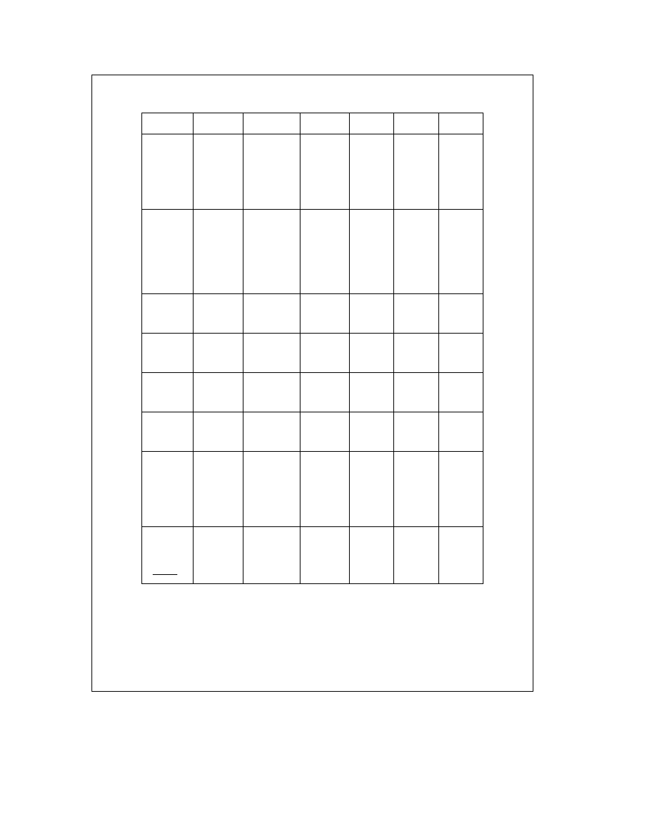
Pinouts for 28- 40- and 44-Pin Packages
Port
Type
Alt Fun
Alt Fun
28-Pin
40-Pin
44-Pin
Pack
Pack
Pack
L0
I O
MIWU
11
17
17
L1
I O
MIWU
12
18
18
L2
I O
MIWU
13
19
19
L3
I O
MIWU
14
20
20
L4
I O
MIWU
T2A
15
21
25
L5
I O
MIWU
T2B
16
22
26
L6
I O
MIWU
17
23
27
L7
I O
MIWU
18
24
28
G0
I O
INT
25
35
39
G1
WDOUT
26
36
40
G2
I O
T1B
27
37
41
G3
I O
T1A
28
38
42
G4
I O
SO
1
3
3
G5
I O
SK
2
4
4
G6
I
SI
3
5
5
G7
I CKO
HALT
4
6
6
RESTART
D0
O
19
25
29
D1
O
20
26
30
D2
O
21
27
31
D3
O
22
28
32
I0
I
7
9
9
I1
I
8
10
10
I2
I
11
11
I3
I
12
12
I4
I
9
13
13
I5
I
10
14
14
I6
I
15
I7
I
16
D4
O
29
33
D5
O
30
34
D6
O
31
35
D7
O
32
36
C0
I O
39
43
C1
I O
40
44
C2
I O
1
1
C3
I O
2
2
C4
I O
21
C5
I O
22
C6
I O
23
C7
I O
24
Unused
16
Unused
15
V
CC
6
8
8
GND
23
33
37
CKI
5
7
7
RESET
24
34
38
e
On the 40-pin package Pins 15 and 16 must be connected to GND
http
www national com
3
Absolute Maximum Ratings
If Military Aerospace specified devices are required
please contact the National Semiconductor Sales
Office Distributors for availability and specifications
Supply Voltage (V
CC
)
7V
Voltage at Any Pin
b
0 3V to V
CC
a
0 3V
Total Current into V
CC
Pin (Source)
100 mA
Total Current out of GND Pin (Sink)
110 mA
Storage Temperature Range
b
65 C to
a
140 C
Note
Absolute maximum ratings indicate limits beyond
which damage to the device may occur DC and AC electri-
cal specifications are not ensured when operating the de-
vice at absolute maximum ratings
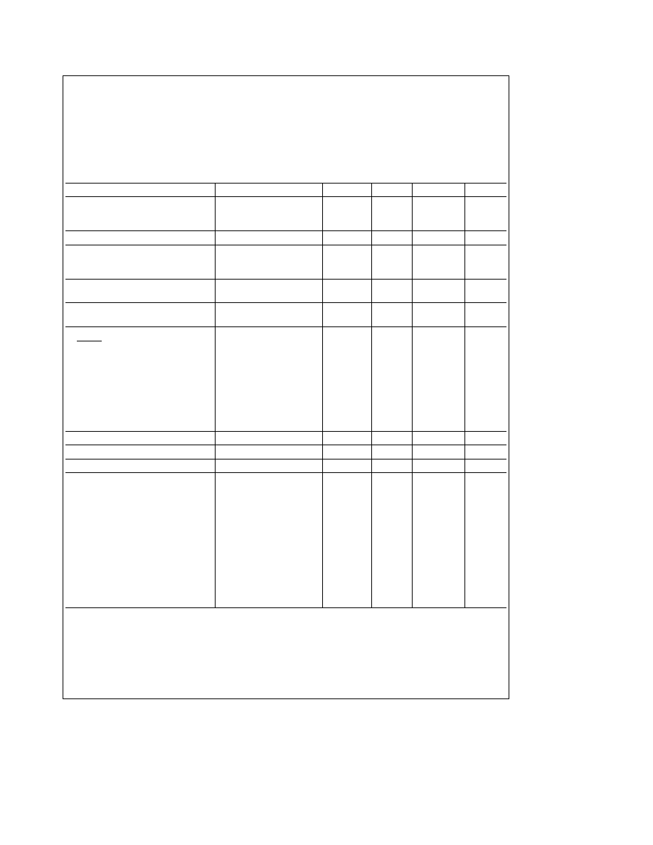
DC Electrical Characteristics
COP98XCL 0 C
s
T
A
s
a
70 C unless otherwise specified
Parameter
Conditions
Min
Typ
Max
Units
Operating Voltage
COP98XCL
2 5
4 0
V
COP98XCLH
4 0
6 0
V
Power Supply Ripple (Note 1)
Peak-to-Peak
0 1 V
CC
V
Supply Current (Note 2)
CKI
e
10 MHz
V
CC
e
6V t
c
e
1 ms
12 5
mA
CKI
e
4 MHz
V
CC
e
4V t
c
e
2 5 ms
2 5
mA
HALT Current (Note 3)
V
CC
e
6V CKI
e
0 MHz
k
0 7
8
m
A
V
CC
e
4V CKI
e
0 MHz
k
0 4
5
m
A
IDLE Current
CKI
e
10 MHz
V
CC
e
6V t
c
e
1 ms
3 5
mA
Input Levels
RESET
Logic High
0 8 V
CC
V
Logic Low
0 2 V
CC
V
CKI (External and Crystal Osc Modes)
Logic High
0 7 V
CC
V
Logic Low
0 2 V
CC
V
All Other Inputs
Logic High
0 7 V
CC
V
Logic Low
0 2 V
CC
V
Hi-Z Input Leakage
V
CC
e
6V
b
1
a
1
m
A
Input Pullup Current
V
CC
e
6V V
IN
e
0V
b
40
b
250
m
A
G and L Port Input Hysteresis
0 35 V
CC
V
Output Current Levels
D Outputs
Source
V
CC
e
4V V
OH
e
3 3V
b
0 4
mA
V
CC
e
2 5V V
OH
e
1 8V
b
0 2
mA
Sink
V
CC
e
4V V
OL
e
1V
10
mA
V
CC
e
2 5V V
OL
e
0 4V
2 0
mA
All Others
Source (Weak Pull-Up Mode)
V
CC
e
4V V
OH
e
2 7V
b
10
b
100
m
A
V
CC
e
2 5V V
OH
e
1 8V
b
2 5
b
33
m
A
Source (Push-Pull Mode)
V
CC
e
4V V
OH
e
3 3V
b
0 4
mA
V
CC
e
2 5V V
OH
e
1 8V
b
0 2
mA
Sink (Push-Pull Mode)
V
CC
e
4V V
OL
e
0 4V
1 6
mA
V
CC
e
2 5V V
OL
e
0 4V
0 7
mA
Note 1
Rate of voltage change must be less then 0 5 V ms
Note 2
Supply current is measured after running 2000 cycles with a square wave CKI input CKO open inputs at rails and outputs open
Note 3
The HALT mode will stop CKI from oscillating in the RC and the Crystal configurations Test conditions All inputs tied to V
CC
L and G0�G5 configured as
outputs and set high The D port set to zero The clock monitor is disabled
http
www national com
4

DC Electrical Characteristics
0 C
s
T
A
s
a
70 C unless otherwise specified (Continued)
Parameter
Conditions
Min
Typ
Max
Units
TRI-STATE Leakage
V
CC
e
6 0V
b
1
a
1
m
A
Allowable Sink Source
Current per Pin
D Outputs (Sink)
15
mA
All others
3
mA
Maximum Input Current
T
A
e
25 C
g
100
mA
without Latchup (Note 4)
RAM Retention Voltage V
r
500 ns Rise
2
V
and Fall Time (Min)
Input Capacitance
7
pF
Load Capacitance on D2
1000
pF
AC Electrical Characteristics
0 C
s
T
A
s
a
70 C unless otherwise specified
Parameter
Conditions
Min
Typ
Max
Units
Instruction Cycle Time (t
c
)
Crystal or Resonator
4V
s
V
CC
s
6V
1
DC
m
s
2 5V
s
V
CC
k
4V
2 5
DC
m
s
R C Oscillator
4V
s
V
CC
s
6V
3
DC
m
s
2 5V
s
V
CC
k
4V
7 5
DC
m
s
Inputs
t
SETUP
4V
s
V
CC
s
6V
200
ns
2 5V
s
V
CC
k
4V
500
ns
t
HOLD
4V
s
V
CC
s
6V
60
ns
2 5V
s
V
CC
k
4V
150
ns
Output Propagation Delay (Note 5)
R
L
e
2 2k C
L
e
100 pF
t
PD1
t
PD0
SO SK
4V
s
V
CC
s
6V
0 7
m
s
2 5V
s
V
CC
k
4V
1 75
m
s
All Others
4V
s
V
CC
s
6V
1
m
s
2 5V
s
V
CC
k
4V
2 5
m
s
MICROWIRE
TM
Setup Time (t
UWS
)
20
ns
MICROWIRE Hold Time (t
UWH
)
56
ns
MICROWIRE Output Propagation Delay (t
UPD
)
220
ns
Input Pulse Width
Interrupt Input High Time
1
t
c
Interrupt Input Low Time
1
t
c
Timer Input High Time
1
t
c
Timer Input Low Time
1
t
c
Reset Pulse Width
1
m
s
Note 4
Pins G6 and RESET are designed with a high voltage input network for factory testing These pins allow input voltages greater than V
CC
and the pins will
have sink current to V
CC
when biased at voltages greater than V
CC
(the pins do not have source current when biased at a voltage below V
CC
) The effective
resistance to V
CC
is 750X (typical) These two pins will not latch up The voltage at the pins must be limited to less than 14V
Note 5
The output propagation delay is referenced to the end of the instruction cycle where the output change occurs
http
www national com
5