
TL F 5968
CD4046BMCD4046BC
Micropower
Phase-Locked
Loop
November 1995
CD4046BM CD4046BC Micropower Phase-Locked Loop
General Description
The CD4046B micropower phase-locked loop (PLL) con-
sists of a low power linear voltage-controlled oscillator
(VCO) a source follower a zener diode and two phase
comparators The two phase comparators have a common
signal input and a common comparator input The signal
input can be directly coupled for a large voltage signal or
capacitively coupled to the self-biasing amplifier at the sig-
nal input for a small voltage signal
Phase comparator I an exclusive OR gate provides a digital
error signal (phase comp I Out) and maintains 90 phase
shifts at the VCO center frequency Between signal input
and comparator input (both at 50% duty cycle) it may lock
onto the signal input frequencies that are close to harmon-
ics of the VCO center frequency
Phase comparator II is an edge-controlled digital memory
network It provides a digital error signal (phase comp II
Out) and lock-in signal (phase pulses) to indicate a locked
condition and maintains a 0 phase shift between signal in-
put and comparator input
The linear voltage-controlled oscillator (VCO) produces an
output signal (VCO Out) whose frequency is determined by
the voltage at the VCO
IN
input and the capacitor and resis-
tors connected to pin C1
A
C1
B
R1 and R2
The source follower output of the VCO
IN
(demodulator Out)
is used with an external resistor of 10 kX or more
The INHIBIT input when high disables the VCO and source
follower to minimize standby power consumption The zener
diode is provided for power supply regulation if necessary
Features
Y
Wide supply voltage range
3 0V to 18V
Y
Low dynamic
70 mW (typ ) at
power consumption
f
o
e
10 kHz V
DD
e
5V
Y
VCO frequency
1 3 MHz (typ ) at V
DD
e
10V
Y
Low frequency drift
0 06% C at V
DD
e
10V
with temperature
Y
High VCO linearity
1% (typ )
Applications
Y
FM demodulator and modulator
Y
Frequency synthesis and multiplication
Y
Frequency discrimination
Y
Data synchronization and conditioning
Y
Voltage-to-frequency conversion
Y
Tone decoding
Y
FSK modulation
Y
Motor speed control
Block
Connection Diagrams
TL F 5968 � 1
FIGURE 1
Dual-In-Line Package
TL F 5968 � 2
Top View
Order Number CD4046B
C1995 National Semiconductor Corporation
RRD-B30M115 Printed in U S A

Absolute Maximum Ratings
(Notes 1
2)
If Military Aerospace specified devices are required
please contact the National Semiconductor Sales
Office Distributors for availability and specifications
DC Supply Voltage (V
DD
)
b
0 5 to
a
18 V
DC
Input Voltage (V
IN
)
b
0 5 to V
DD
a
0 5 V
DC
Storage Temperature Range (T
S
)
b
65 C to
a
150 C
Power Dissipation (P
D
)
Dual-In-Line
700 mW
Small Outline
500 mW
Lead Temperature (T
L
)
(Soldering 10 seconds)
260 C
Recommended Operating
Conditions
(Note 2)
DC Supply Voltage (V
DD
)
3 to 15 V
DC
Input Voltage (V
IN
)
0 to V
DD
V
DC
Operating Temperature Range (T
A
)
CD4046BM
b
55 C to
a
125 C
CD4046BC
b
40 C to
a
85 C
DC Electrical Characteristics
CD4046BM (Note 2)
Symbol
Parameter
Conditions
b
55 C
a
25 C
a
125 C
Units
Min
Max
Min
Typ
Max
Min
Max
I
DD
Quiescent Device Current
Pin 5
e
V
DD
Pin 14
e
V
DD
Pin 3 9
e
V
SS
V
DD
e
5V
5
0 005
5
150
m
A
V
DD
e
10V
10
0 01
10
300
m
A
V
DD
e
15V
20
0 015
20
600
m
A
Pin 5
e
V
DD
Pin 14
e
Open
Pin 3 2
e
V
SS
V
DD
e
5V
45
5
35
185
m
A
V
DD
e
10V
450
20
350
650
m
A
V
DD
e
15V
1200
50
900
1500
m
A
V
OL
Low Level Output Voltage V
DD
e
5V
0 05
0
0 05
0 05
V
V
DD
e
10V
0 05
0
0 05
0 05
V
V
DD
e
15V
0 05
0
0 05
0 05
V
V
OH
High Level Output Voltage V
DD
e
5V
4 95
4 95
5
4 95
V
V
DD
e
10V
9 95
9 95
10
9 95
V
V
DD
e
15V
14 95
14 95
15
14 95
V
V
IL
Low Level Input Voltage
V
DD
e
5V V
O
e
0 5V or 4 5V
1 5
2 25
1 5
1 5
V
Comparator and Signal In
V
DD
e
10V V
O
e
1V or 9V
3 0
4 5
3 0
3 0
V
V
DD
e
15V V
O
e
1 5V or 13 5V
4 0
6 25
4 0
4 0
V
V
IH
High Level Input Voltage
V
DD
e
5V V
O
e
0 5V or 4 5V
3 5
3 5
2 75
3 5
V
Comparator and Signal In
V
DD
e
10V V
O
e
1V or 9V
7 0
7 0
5 5
7 0
V
V
DD
e
15V V
O
e
1 5V or 13 5V
11 0
11 0
8 25
11 0
V
I
OL
Low Level Output Current
V
DD
e
5V V
O
e
0 4V
0 64
0 51
0 88
0 36
mA
(Note 4)
V
DD
e
10V V
O
e
0 5V
1 6
1 3
2 25
0 9
mA
V
DD
e
15V V
O
e
1 5V
4 2
3 4
8 8
2 4
mA
I
OH
High Level Output Current V
DD
e
5V V
O
e
4 6V
b
0 64
b
0 51
b
0 88
b
0 36
mA
(Note 4)
V
DD
e
10V V
O
e
9 5V
b
1 6
b
1 3
b
2 25
b
0 9
mA
V
DD
e
15V V
O
e
13 5V
b
4 2
b
3 4
b
8 8
b
2 4
mA
I
IN
Input Current
All Inputs Except Signal Input
V
DD
e
14V V
IN
e
0V
b
0 1
b
10
b
5
b
0 1
b
1 0
m
A
V
DD
e
15V V
IN
e
15V
0 1
10
b
5
0 1
1 0
m
A
C
IN
Input Capacitance
Any Input (Note 3)
7 5
pF
P
T
Total Power Dissipation
f
o
e
10 kHz R1
e
1 MX
R2
e
%
VCO
IN
e
V
DD
2
V
DD
e
5V
0 07
mW
V
DD
e
10V
0 6
mW
V
DD
e
15V
2 4
mW
2
DC Electrical Characteristics
CD4046BC (Note 2)
Symbol
Parameter
Conditions
b
40 C
a
25 C
a
85 C
Units
Min
Max
Min
Typ
Max
Min
Max
I
DD
Quiescent Device Current
Pin 5
e
V
DD
Pin 14
e
V
DD
Pin 3 9
e
V
SS
V
DD
e
5V
20
0 005
20
150
m
A
V
DD
e
10V
40
0 01
40
300
m
A
V
DD
e
15V
80
0 015
80
600
m
A
Pin 5
e
V
DD
Pin 14
e
Open
Pin 3 9
e
V
SS
V
DD
e
5V
70
5
55
205
m
A
V
DD
e
10V
530
20
410
710
m
A
V
DD
e
15V
1500
50
1200
1800
m
A
V
OL
Low Level Output Voltage V
DD
e
5V
0 05
0
0 05
0 05
V
V
DD
e
10V
0 05
0
0 05
0 05
V
V
DD
e
15V
0 05
0
0 05
0 05
V
V
OH
High Level Output Voltage V
DD
e
5V
4 95
4 95
5
4 95
V
V
DD
e
10V
9 95
9 95
10
9 95
V
V
DD
e
15V
14 95
14 95
15
14 95
V
V
IL
Low Level Input Voltage
V
DD
e
5V V
O
e
0 5V or 4 5V
1 5
2 25
1 5
1 5
V
Comparator and Signal In
V
DD
e
10V V
O
e
1V or 9V
3 0
4 5
3 0
3 0
V
V
DD
e
15V V
O
e
1 5V or 13 5V
4 0
6 25
4 0
4 0
V
V
IH
High Level Input Voltage
V
DD
e
5V V
O
e
0 5V or 4 5V
3 5
3 5
2 75
3 5
V
Comparator and Signal In
V
DD
e
10V V
O
e
1V or 9V
7 0
7 0
5 5
7 0
V
V
DD
e
15V V
O
e
1 5V or 13 5V
11 0
11 0
8 25
11 0
V
I
OL
Low Level Output Current
V
DD
e
5V V
O
e
0 4V
0 52
0 44
0 88
0 36
mA
(Note 4)
V
DD
e
10V V
O
e
0 5V
1 3
1 1
2 25
0 9
mA
V
DD
e
15V V
O
e
1 5V
3 6
3 0
8 8
2 4
mA
I
OH
High Level Output Current V
DD
e
5V V
O
e
4 6V
b
0 52
b
0 44
b
0 88
b
0 36
mA
(Note 4)
V
DD
e
10V V
O
e
9 5V
b
1 3
b
1 1
b
2 25
b
0 9
mA
V
DD
e
15V V
O
e
13 5V
b
3 6
b
3 0
b
8 8
b
2 4
mA
I
IN
Input Current
All Inputs Except Signal Input
V
DD
e
15V V
IN
e
0V
b
0 3
b
10
b
5
b
0 3
b
1 0
m
A
V
DD
e
15V V
IN
e
15V
0 3
10
b
5
0 3
1 0
m
A
C
IN
Input Capacitance
Any Input (Note 3)
7 5
pF
P
T
Total Power Dissipation
f
o
e
10 kHz R1
e
1 MX
R2
e
%
VCO
IN
e
V
DD
2
V
DD
e
5V
0 07
mW
V
DD
e
10V
0 6
mW
V
DD
e
15V
2 4
mW
Note 1
``Absolute Maximum Ratings'' are those values beyond which the safety of the device cannot be guaranteed They are not meant to imply that the devices
should be operated at these limits The table of ``Recommended Operating Conditions'' and ``Electrical Characteristics'' provides conditions for actual device
operation
Note 2
V
SS
e
0V unless otherwise specified
Note 3
Capacitance is guaranteed by periodic testing
Note 4
I
OH
and I
OL
are tested one output at a time
3
AC Electrical Characteristics
CD4046BM CD4046BC T
A
e
25 C C
L
e
50 pF
Symbol
Parameter
Conditions
Min
Typ
Max
Units
VCO SECTION
I
DD
Operating Current
f
o
e
10 kHz R1
e
1 MX
R2
e
%
VCO
IN
e
V
DD
2
V
DD
e
5V
20
m
A
V
DD
e
10V
90
m
A
V
DD
e
15V
200
m
A
f
MAX
Maximum Operating Frequency
C1
e
50 pF R1
e
10 kX
R2
e
%
VCO
IN
e
V
DD
V
DD
e
5V
0 4
0 8
MHz
V
DD
e
10V
0 6
1 2
MHz
V
DD
e
15V
1 0
1 6
MHz
Linearity
VCO
IN
e
2 5V
g
0 3V
R1
t
10 kX V
DD
e
5V
1
%
VCO
IN
e
5V
g
2 5V
R1
t
400 kX V
DD
e
10V
1
%
VCO
IN
e
7 5V
g
5V
R1
t
1 MX V
DD
e
15V
1
%
Temperature-Frequency Stability
% C*1 f V
DD
No Frequency Offset f
MIN
e
0
R2
e
%
V
DD
e
5V
0 12 � 0 24
% C
V
DD
e
10V
0 04 � 0 08
% C
V
DD
e
15V
0 015 � 0 03
% C
Frequency Offset f
MIN
i
0
V
DD
e
5V
0 06 � 0 12
% C
V
DD
e
10V
0 05 � 0 1
% C
V
DD
e
15V
0 03 � 0 06
% C
VCO
IN
Input Resistance
V
DD
e
5V
10
6
MX
V
DD
e
10V
10
6
MX
V
DD
e
15V
10
6
MX
VCO
Output Duty Cycle
V
DD
e
5V
50
%
V
DD
e
10V
50
%
V
DD
e
15V
50
%
t
THL
VCO Output Transition Time
V
DD
e
5V
90
200
ns
t
THL
V
DD
e
10V
50
100
ns
V
DD
e
15V
45
80
ns
AC Parameters are guaranteed by DC correlated testing
4
AC Electrical Characteristics
CD4046BM CD4046BC T
A
e
25 C C
L
e
50 pF (Continued)
Symbol
Parameter
Conditions
Min
Typ
Max
Units
PHASE COMPARATORS SECTION
R
IN
Input Resistance
Signal Input
V
DD
e
5V
1
3
MX
V
DD
e
10V
0 2
0 7
MX
V
DD
e
15V
0 1
0 3
MX
Comparator Input
V
DD
e
5V
10
6
MX
V
DD
e
10V
10
6
MX
V
DD
e
15V
10
6
MX
AC-Coupled Signal Input Voltage
C
SERIES
e
1000 pF
Sensitivity
f
e
50 kHz
V
DD
e
5V
200
400
mV
V
DD
e
10V
400
800
mV
V
DD
e
15V
700
1400
mV
DEMODULATOR OUTPUT
VCO
IN
b
Offset Voltage
RS
t
10 kX V
DD
e
5V
1 50
2 2
V
V
DEM
RS
t
10 kX V
DD
e
10V
1 50
2 2
V
RS
t
50 kX V
DD
e
15V
1 50
2 2
V
Linearity
RS
t
50 kX
VCO
IN
e
2 5V
g
0 3V V
DD
e
5V
0 1
%
VCO
IN
e
5V
g
2 5V V
DD
e
10V
0 6
%
VCO
IN
e
7 5V
g
5V V
DD
e
15V
0 8
%
ZENER DIODE
V
Z
Zener Diode Voltage
I
Z
e
50 mA
6 3
7 0
7 7
V
R
Z
Zener Dynamic Resistance
I
Z
e
1 mA
100
X
AC Parameters are guaranteed by DC correlated testing
5
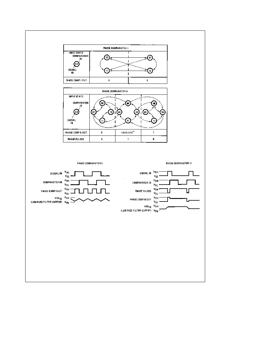
Phase Comparator State Diagrams
TL F 5968 � 3
FIGURE 2
Typical Waveforms
TL F 5968 � 4
FIGURE 3 Typical Waveform Employing Phase
Comparator I in Locked Condition
TL F 5968 � 5
FIGURE 4 Typical Waveform Employing Phase
Comparator II in Locked Condition
6

Typical Performance Characteristics
for R1
e
10 kX 100 kX and 1 MX
Typical Center Frequency vs C1
TL F 5968 � 6
FIGURE 5a
Typical Frequency vs C1
for R2
e
10 kX 100 kX and 1 MX
TL F 5968 � 13
FIGURE 5b
Note
To obtain approximate total power dissipation of PLL system for no-signal input Phase Comparator I P
D
(Total)
e
P
D
(f
o
)
a
P
D
(f
MIN
)
a
P
D
(R
S
) Phase
Comparator II P
D
(Total)
e
P
D
(f
MIN
)
7

Typical Performance Characteristics
(Continued)
Typical f
MAX
f
MIN
vs R2 R1
TL F 5968 � 14
FIGURE 5C
Typical VCO Power Dissipation
at Center Frequency vs R1
TL F 5968 � 15
FIGURE 6a
Note
To obtain approximate total power dissipation of PLL system for no-signal input Phase Comparator I P
D
(Total)
e
P
D
(f
o
)
a
P
D
(f
MIN
)
a
P
D
(R
S
) Phase
Comparator II P
D
(Total)
e
P
D
(f
MIN
)
8

Typical Performance Characteristics
(Continued)
Typical VCO Power Dissipation at f
MIN
vs R2
TL F 5968 � 16
FIGURE 6b
Typical Source Follower Power Dissipation vs R
S
TL F 5968 � 17
FIGURE 6c
Note
To obtain approximate total power dissipation of PLL system for no-signal input Phase Comparator I P
D
(Total)
e
P
D
(f
o
)
a
P
D
(f
MIN
)
a
P
D
(R
S
) Phase
Comparator II P
D
(Total)
e
P
D
(f
MIN
)
9
Typical Performance Characteristics
(Continued)
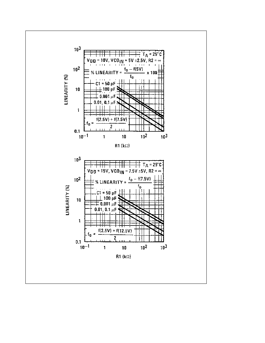
TL F 5968 � 18
TL F 5968 � 19
FIGURE 7 Typical VCO Linearity vs R1 and C1
Note
To obtain approximate total power dissipation of PLL system for no-signal input Phase Comparator I P
D
(Total)
e
P
D
(f
o
)
a
P
D
(f
MIN
)
a
P
D
(R
S
) Phase
Comparator II P
D
(Total)
e
P
D
(f
MIN
)
10

Design Information
This information is a guide for approximating the value of
external components for the CD4046B in a phase-locked-
loop system The selected external components must be
within the following ranges R1 R2
t
10 kX R
S
t
10 kX
C1
t
50 pF
In addition to the given design information refer to
Figure 5
for R1 R2 and C1 component selections
Using Phase Comparator I
Using Phase Comparator II
Characteristics
VCO Without Offset
VCO With Offset
VCO Without Offset
VCO With Offset
R2
e
%
R2
e
%
VCO Frequency
For No Signal Input
VCO in PLL system will adjust
VCO in PLL system will adjust to
to center frequency f
o
lowest operating frequency f
min
Frequency Lock
2 f
L
e
full VCO frequency range
Range 2 f
L
2 f
L
e
f
max
b
f
min
Frequency Capture
Range 2 f
C
2 f
C
1
q
0
2
q
f
L
u
1
Loop Filter
f
C
e
f
L
Component
Selection
For 2 f
C
see Ref
Phase Angle Between
90 at center frequency (f
o
) approximating
Always 0 in lock
Single and Comparator
0 and 180 at ends of lock range (2 f
L
)
Locks on Harmonics
Yes
No
of Center Frequency
Signal Input Noise
High
Low
Rejection
VCO Component
Given f
o
Given f
o
and f
L
Given f
max
Given f
min
and f
max
Selection
Use f
o
with
Calculate f
min
Calculate f
o
from
Use f
min
with
Figure 5a to
from the equation
the equation
Figure 5b to
determine R1
determine R2 and C1
f
min
e
f
o
b
f
L
and C1
f
o
e
f
max
2
Use f
min
with
Figure 5b
Calculate
f
max
f
min
to determine R2 and C1
Use f
o
with
Figure 5a to
determine R1 and C1
Use
f
max
f
min
with
Figure 5c
Calculate
f
max
f
min
to determine ratio
from the equation
R2 R1 to obtain R1
f
max
f
min
e
f
o
a
f
L
f
o
b
f
L
Use
f
max
f
min
with
Figure 5c
to determine ratio R2
R1 to obtain R1
TL F 5968 � 7
TL F 5968 � 9
TL F 5968 � 10
TL F 5968 � 8
TL F 5968 � 11
TL F 5968 � 12
References
G S Moschytz ``Miniaturized RC Filters Using Phase-Locked Loop'' BSTJ May 1965
Floyd Gardner ``Phaselock Techniques'' John Wiley
Sons 1966
11

12

Physical Dimensions
inches (millimeters)
Order Number CD4046BMJ or CD4046BCJ
NS Package Number J16A
13

CD4046BMCD4046BC
Micropower
Phase-Locked
Loop
Physical Dimensions
inches (millimeters) (Continued)
Order Number CD4046BMN or CD4046BCN
NS Package Number N16E
LIFE SUPPORT POLICY
NATIONAL'S PRODUCTS ARE NOT AUTHORIZED FOR USE AS CRITICAL COMPONENTS IN LIFE SUPPORT
DEVICES OR SYSTEMS WITHOUT THE EXPRESS WRITTEN APPROVAL OF THE PRESIDENT OF NATIONAL
SEMICONDUCTOR CORPORATION As used herein
1 Life support devices or systems are devices or
2 A critical component is any component of a life
systems which (a) are intended for surgical implant
support device or system whose failure to perform can
into the body or (b) support or sustain life and whose
be reasonably expected to cause the failure of the life
failure to perform when properly used in accordance
support device or system or to affect its safety or
with instructions for use provided in the labeling can
effectiveness
be reasonably expected to result in a significant injury
to the user
National Semiconductor
National Semiconductor
National Semiconductor
National Semiconductor
Corporation
Europe
Hong Kong Ltd
Japan Ltd
1111 West Bardin Road
Fax (a49) 0-180-530 85 86
13th Floor Straight Block
Tel 81-043-299-2309
Arlington TX 76017
Email cnjwge tevm2 nsc com
Ocean Centre 5 Canton Rd
Fax 81-043-299-2408
Tel 1(800) 272-9959
Deutsch Tel (a49) 0-180-530 85 85
Tsimshatsui Kowloon
Fax 1(800) 737-7018
English
Tel (a49) 0-180-532 78 32
Hong Kong
Fran ais Tel (a49) 0-180-532 93 58
Tel (852) 2737-1600
Italiano
Tel (a49) 0-180-534 16 80
Fax (852) 2736-9960
National does not assume any responsibility for use of any circuitry described no circuit patent licenses are implied and National reserves the right at any time without notice to change said circuitry and specifications