TL F 5942
CD4006BMCD4006BC
18-Stage
Static
Shift
Register
February 1988
CD4006BM CD4006BC 18-Stage Static Shift Register
General Description
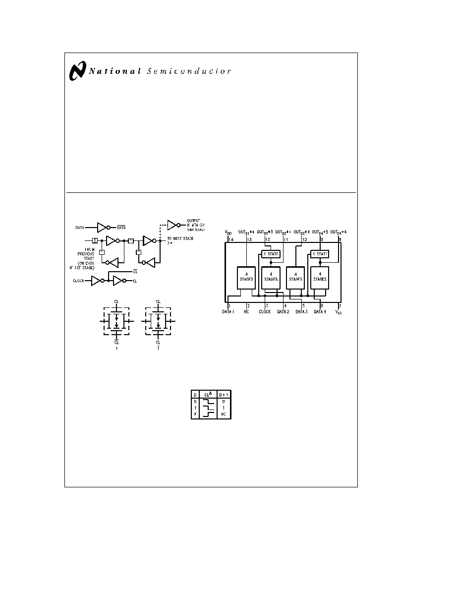
The CD4006BM CD4006BC 18-stage static shift register is
comprised of four separate shift register sections two sec-
tions of four stages and two sections of five stages Each
section has an independent data input Outputs are avail-
able at the fourth stage and the fifth stage of each section
A common clock signal is used for all stages Data is shifted
to the next stage on the negative-going transition of the
clock Through appropriate connections of inputs and out-
puts multiple register sections of 4 5 8 and 9 stages or
single register sections of 10 12 13 14 16 17 and 18
stages can be implemented using one package
Features
Y
Wide supply voltage range
3 0V to 15V
Y
High noise immunity
0 45 V
DD
(typ )
Y
Low power TTL
fan out of 2 driving 74L
compatibility
or 1 driving 74LS
Y
Low clock input capacitance
6 pF (typ )
Y
Medium speed
10 MHz (typ ) (with V
DD
e
10V)
Y
Low power
Y
Fully static operation
Logic Diagrams
TL F 5942 Ł 1
TL F 5942 Ł 3
Connection Diagram
Dual-In-Line Package
TL F 5942 Ł 2
Top View
Order Number CD4006B
Truth Table
TL F 5942 Ł 4
X
e
Don't care
D
e
Level change
NC
e
No change
C1995 National Semiconductor Corporation
RRD-B30M105 Printed in U S A

Absolute Maximum Ratings
(Notes 1 and 2)
If Military Aerospace specified devices are required
please contact the National Semiconductor Sales
Office Distributors for availability and specifications
DC Supply Voltage (V
DD
)
b
0 5 to
a
18 V
DC
Input Voltage (V
IN
)
b
0 5 to V
DD
a
0 5 V
DC
Storage Temperature Range (T
S
)
b
65 C to
a
150 C
Power Dissipation (P
D
)
Dual-In-Line
700 mW
Small Outline
500 mW
Lead Temperature (T
L
)
(Soldering 10 seconds)
260 C
Recommended Operating
Conditions
(Note 2)
DC Supply Voltage (V
DD
)
a
3 0V to
a
15V
Input Voltage (V
IN
)
0V to V
DD
V
DC
Operating Temperature Range (T
A
)
CD4006BM
b
55 C to
a
125 C
CD4006BC
b
40 C to
a
85 C
DC Electrical Characteristics
CD4006BM (Note 2)
Symbol
Parameter
Conditions
b
55 C
a
25 C
a
125 C
Units
Min
Max
Min
Typ
Max
Min
Max
I
DD
Quiescent
V
DD
e
5 0V V
IN
e
V
DD
or V
SS
5 0
0 005
5 0
150
m
A
Device Current
V
DD
e
10V V
IN
e
V
DD
or V
SS
10
0 010
10
300
m
A
V
DD
e
15V V
IN
e
V
DD
or V
SS
20
0 015
20
600
m
A
V
OL
Low Level
V
DD
e
5 0V
0 05
0
0 05
0 05
V
Output Voltage
V
DD
e
10V
0 05
0
0 05
0 05
V
V
DD
e
15V
0 05
0
0 05
0 05
V
V
OH
High Level
V
DD
e
5 0V
4 95
4 95
5 0
4 95
V
Output Voltage
V
DD
e
10V
9 95
9 95
10
9 95
V
V
DD
e
15V
14 95
14 95
15
14 95
V
V
IL
Low Level
V
DD
e
5 0V V
O
e
0 5V or 4 5V
1 5
2 25
1 5
1 5
V
Input Voltage
V
DD
e
10V V
O
e
1 0V or 9 0V
3 0
4 50
3 0
3 0
V
V
DD
e
15V V
O
e
1 5V or 13 5V
4 0
6 75
4 0
4 0
V
V
IH
High Level
V
DD
e
5 0V V
O
e
0 5V or 4 5V
3 5
3 5
2 75
3 5
V
Input Voltage
V
DD
e
10V V
O
e
1 0V or 9 0V
7 0
7 0
5 50
7 0
V
V
DD
e
15V V
O
e
1 5V or 13 5V
11 0
11 0
8 25
11 0
V
I
OL
Low Level
V
DD
e
5 0V V
O
e
0 4V
0 64
0 51
0 88
0 36
mA
Output Current
V
DD
e
10V V
O
e
0 5V
1 6
1 3
2 25
0 9
mA
(Note 3)
V
DD
e
15V V
O
e
1 5V
4 2
3 4
8 8
2 4
mA
I
OH
High Level
V
DD
e
5 0V V
O
e
4 6V
b
0 64
b
0 51
b
0 88
b
0 36
mA
Output Current
V
DD
e
10V V
O
e
9 5V
b
1 6
b
1 3
b
2 25
b
0 9
mA
(Note 3)
V
DD
e
15V V
O
e
13 5V
b
4 2
b
3 4
b
8 8
b
2 4
mA
I
IN
Input Current
V
DD
e
15V V
IN
e
0V
b
0 1
b
0 1
b
10
b
5
b
1 0
m
A
V
DD
e
15V V
IN
e
15V
0 1
10
b
5
0 1
1 0
m
A
DC Electrical Characteristics
CD4006BC (Note 2)
Symbol
Parameter
Conditions
b
40 C
a
25 C
a
85 C
Units
Min
Max
Min
Typ
Max
Min
Max
I
DD
Quiescent
V
DD
e
5 0V V
IN
e
V
DD
or V
SS
20
0 005
20
150
m
A
Device Current
V
DD
e
10V V
IN
e
V
DD
or V
SS
40
0 010
40
300
m
A
V
DD
e
15V V
IN
e
V
DD
or V
SS
80
0 015
80
600
m
A
V
OL
Low Level
V
DD
e
5 0V
0 05
0
0 05
0 05
V
Output Voltage
V
DD
e
10V
0 05
0
0 05
0 05
V
V
DD
e
15V
0 05
0
0 05
0 05
V
V
OH
High Level
V
DD
e
5 0V
4 95
4 95
5 0
4 95
V
Output Voltage
V
DD
e
10V
9 95
9 95
10
9 95
V
V
DD
e
15V
14 95
14 95
15
14 95
V
2

DC Electrical Characteristics
CD4006BC (Note 2) (Continued)
Symbol
Parameter
Conditions
b
40 C
a
25 C
a
85 C
Units
Min
Max
Min
Typ
Max
Min
Max
V
IL
Low Level
V
DD
e
5 0V V
O
e
0 5V or 4 5V
1 5
2 25
1 5
1 5
V
Input Voltage
V
DD
e
10V V
O
e
1 0V or 9 0V
3 0
4 5
3 0
3 0
V
V
DD
e
15V V
O
e
1 5V or 13 5V
4 0
6 75
4 0
4 0
V
V
IH
High Level
V
DD
e
5 0V V
O
e
0 5V or 4 5V
3 5
3 5
2 75
3 5
V
Input Voltage
V
DD
e
10V V
O
e
1 0V or 9 0V
7 0
7 0
5 5
7 0
V
V
DD
e
15V V
O
e
1 5V or 13 5V
11
11
8 25
11
V
I
OL
Low Level
V
DD
e
5 0V V
O
e
0 4V
0 52
0 44
0 88
0 36
mA
Output Current
V
DD
e
10V V
O
e
0 5V
1 3
1 1
2 25
0 9
mA
(Note 3)
V
DD
e
15V V
O
e
1 5V
3 6
3 0
8 8
2 4
mA
I
OH
High Level
V
IL
e
0V V
IH
e
V
DD
Output Current
V
DD
e
5 0V V
O
e
4 6V
b
0 52
b
0 44
b
0 88
b
0 36
mA
(Note 3)
V
DD
e
10V V
O
e
9 5V
b
1 3
b
1 1
b
2 25
b
0 9
mA
V
DD
e
15V V
O
e
13 5V
b
3 6
b
3 0
b
8 8
b
2 4
mA
I
IN
Input Current
V
DD
e
15V V
IN
e
0V
b
0 3
b
10
b
5
b
0 3
b
1 0
m
A
V
DD
e
15V V
IN
e
15V
0 3
10
b
5
0 3
1 0
m
A
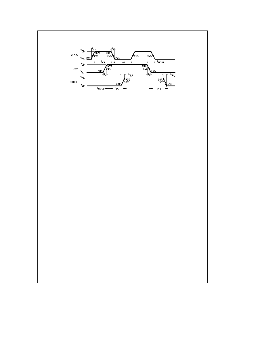
AC Electrical Characteristics
CD4006BM CD4006BC T
A
e
25 C C
L
e
50 pF unless otherwise noted
Symbol
Parameter
Conditions
Min
Typ
Max
Units
t
PLH
t
PHL
Propagation Delay Time (t
PLH
e
t
PHL
)
V
DD
e
5 0V
200
400
ns
V
DD
e
10V
100
200
ns
V
DD
e
15V
80
150
ns
t
TLH
t
THL
Transition Time (t
TLH
e
t
THL
)
V
DD
e
5 0V
100
200
ns
V
DD
e
10V
50
100
ns
V
DD
e
15V
40
80
ns
t
WL
t
WH
Minimum Clock Pulse Width (t
WL
e
t
WH
)
V
DD
e
5 0V
100
200
ns
V
DD
e
10V
45
100
ns
V
DD
e
15V
35
70
ns
t
RCL
t
FCL
Clock Rise and Fall Time (t
RCL
e
t
FCL
)
V
DD
e
5 0V
15
m
s
V
DD
e
10V
15
m
s
V
DD
e
15V
15
m
s
t
SU
Minimum Set-Up Time
V
DD
e
5 0V
50
100
ns
V
DD
e
10V
25
50
ns
V
DD
e
15V
20
40
ns
t
H
Minimum Hold Time
V
DD
e
5 0V
55
110
ns
V
DD
e
10V
35
70
ns
V
DD
e
15V
30
60
ns
f
CL
Maximum Clock Frequency
V
DD
e
5 0V
2 5
5 0
MHz
V
DD
e
10V
5 0
12
MHz
V
DD
e
15V
7 0
16
MHz
C
L
Input Capacitance
Data Input
5 0
pF
CLK Input
7 5
pF
AC Parameters are guaranteed by DC correlated testing
Note 1
``Absolute Maximum Ratings'' are those values beyond which the safety of the device cannot be guaranteed they are not meant to imply that the devices
should be operated at these limits The tables of ``Recommended Operating Conditions'' and ``Electrical Characteristics'' provide conditions for actual device
operation
Note 2
V
SS
e
0V unless otherwise specified
Note 3
I
OL
and I
OH
are tested one output at a time
3