ADC12762
12-Bit, 1.4 MHz, 300 mW A/D Converter
with Input Multiplexer and Sample/Hold
General Description
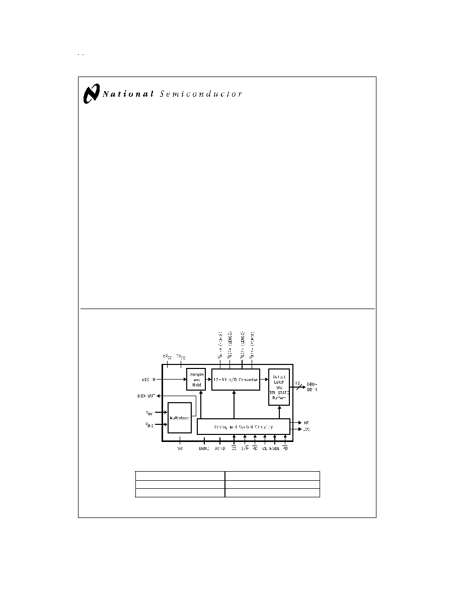
Using an innovative multistep conversion technique, the
12-bit ADC12762 CMOS analog-to-digital converter digitizes
signals at a 1.4 MHz sampling rate while consuming a maxi-
mum of only 300 mW on a single +5V supply. The
ADC12762
performs
a
12-bit
conversion
in
three
lower-resolution "flash" conversions, yielding a fast A/D with-
out the cost and power dissipation associated with true flash
approaches.
The analog input voltage to the ADC12762 is tracked and
held by an internal sampling circuit, allowing high frequency
input signals to be accurately digitized without the need for
an external sample-and-hold circuit. The ADC12762 features
two sample-and-hold/flash comparator sections which allow
the converter to acquire one sample while converting the
previous. This pipelining technique increases conversion
speed without sacrificing performance. The multiplexer out-
put is available to the user in order to perform additional ex-
ternal signal processing before the signal is digitized.
When the converter is not digitizing signals, it can be placed
in the Standby mode; typical power consumption in this
mode is 250 µW.
Features
n
Built-in sample-and-hold
n
Single +5V supply
n
Single channel or 2 channel multiplexer operation
Key Specifications
n
Sampling rate
1.4 MHz (min)
n
Conversion time
593 ns (typ)
n
SNR, f
IN
= 100 kHz
67.5 dB (min)
n
Power dissipation (f
s
= 1.4 MHz)
300 mW (max)
n
No missing codes over temperature
Guaranteed
Applications
n
CCD image scanners
n
Digital signal processor front ends
n
Instrumentation
n
Disk drives
n
Mobile telecommunications
n
Waveform digitizers
ADC12762 Block Diagram
Ordering Information
Commercial (0°C
T
A
+70°C)
Package
ADC12762CCV
V44 Plastic Leaded Chip Carrier
ADC12062EVAL
Evaluation Board
TRI-STATE
®
is a registered trademark of National Semiconductor Corporation.
DS012811-1
June 1999
ADC12762
12-Bit,
1.4
MHz,
300
mW
A/D
Converter
with
Input
Multiplexer
and
Sample/Hold
© 1999 National Semiconductor Corporation
DS012811
www.national.com

Absolute Maximum Ratings
(Notes 1, 2)
If Military/Aerospace specified devices are required,
please contact the National Semiconductor Sales Office/
Distributors for availability and specifications.
Supply Voltage (V
CC
= DV
CC
= AV
CC
)
-0.3V to +6V
Voltage at Any Input or Output
-0.3V to V
CC
+ 0.3V
Input Current at Any Pin (Note 3)
25 mA
Package Input Current (Note 3)
50 mA
Power Dissipation (Note 4)
ADC12762CCV
875 mW
ESD Susceptibility (Note 5)
2000V
Soldering Information (Note 6)
V Package, Infrared, 15 seconds
+300°C
Storage Temperature Range
-65°C to +150°C
Maximum Junction Temperature (T
JMAX
)
150°C
Operating Ratings
(Notes 1, 2)
Temperature Range
T
MIN
T
A
T
MAX
ADC12762CCV
-0°C
T
A
+70°C
Supply Voltage Range (DV
CC
= AV
CC
)
4.75V to 5.25V
Converter Characteristics
The following specifications apply for DV
CC
= AV
CC
= +5V, V
REF+(SENSE)
= +4.096V, V
REF-(SENSE)
= AGND, and f
s
=
1.4 MHz, unless otherwise specified. Boldface limits apply for T
A
= T
J
from T
MIN
to T
MAX
; all other limits T
A
= T
J
= +25°C.
Symbol
Parameter
Conditions
Typ
Limit
Units
(Note 7)
(Note 8)
(Limit)
Resolution
12
Bits
Differential Linearity Error
T
MIN
to T
MAX
±
0.4
±
0.95
LSB (max)
Integral Linearity Error
T
MIN
to T
MAX
±
0.4
±
2.0
LSB (max)
(Note 9)
Offset Error
T
MIN
to T
MAX
±
0.3
±
4.0
LSB (max)
Full-Scale Error
T
MIN
to T
MAX
±
0.3
±
4.0
LSB (max)
Power Supply Sensitivity
DV
CC
= AV
CC
= 5V
±
5%
±
0.75
LSB (max)
(Note 15)
R
REF
Reference Resistance
940
500
(min)
1300
(max)
V
REF(+)
V
REF+(SENSE)
Input Voltage
AV
CC
V (max)
V
REF(-)
V
REF-(SENSE)
Input Voltage
AGND
V (min)
V
IN
Input Voltage Range
To V
IN1
, V
IN2
, or ADC IN
AV
CC
+0.05V
V (max)
AGND - 0.05V
V (min)
ADC IN Input Leakage
AGND to AV
CC
- 0.3V
0.1
3
µA (max)
C
ADC
ADC IN Input Capacitance
25
pF
MUX On-Channel Leakage
AGND to AV
CC
- 0.3V
0.1
3
µA (max)
MUX Off-Channel Leakage
AGND to AV
CC
- 0.3V
0.1
3
µA (max)
C
MUX
Multiplexer Input Cap
7
pF
MUX Off Isolation
f
IN
= 100 kHz
92
dB
Dynamic Characteristics
(Note 10)
The following specifications apply for DV
CC
= AV
CC
= +5V, V
REF+(SENSE)
= +4.096V, V
REF-(SENSE)
= AGND, R
S
= 25
, f
IN
=
100 kHz, 0 dB from fullscale, and f
s
= 1.4 MHz, unless otherwise specified. Boldface limits apply for T
A
= T
J
from T
MIN
to
T
MAX
; all other limits T
A
= T
J
= +25°C.
Symbol
Parameter
Conditions
Typ
Limit
Units
(Note 7)
(Note 8)
(Limit)
SINAD
Signal-to-Noise Plus
T
MIN
to T
MAX
70
67.0
dB (min)
Distortion Ratio
SNR
Signal-to-Noise Ratio
T
MIN
to T
MAX
70
67.5
dB (min)
(Note 11)
THD
Total Harmonic Distortion
T
MIN
to T
MAX
-80
-70
dBc (max)
(Note 12)
ENOB
Effective Number of Bits
T
MIN
to t
MAX
11.3
10.8
Bits (min)
(Note 13)
IMD
Intermodulation Distortion
f
IN
= 88.7 kHz, 89.5 kHz
-80
dBc
www.national.com
2
DC Electrical Characteristics
The following specifications apply for DV
CC
= AV
CC
= +5V, V
REF+(SENSE)
= +4.096V, V
REF-(SENSE)
= AGND, and f
s
=
1.4 MHz, unless otherwise specified. Boldface limits apply for T
A
= T
J
from T
MIN
to T
MAX
; all other limits T
A
= T
J
= +25°C.
Symbol
Parameter
Conditions
Typ
Limit
Units
(Note 7)
(Note 8)
(Limit)
V
IN(1)
Logical "1" Input Voltage
DV
CC
= AV
CC
= +5.5V
2.0
V (min)
V
IN(0)
Logical "0" Input Voltage
DV
CC
= AV
CC
= +4.5V
0.8
V (max)
I
IN(1)
Logical "1" Input Current
0.1
1.0
µA (max)
I
IN(0)
Logical "0" Input Current
0.1
1.0
µA (max)
V
OUT(1)
Logical "1" Output Voltage
DV
CC
= AV
CC
= +4.5V,
I
OUT
= -360 µA
2.4
V (min)
I
OUT
= -100 µA
4.25
V (min)
V
OUT(0)
Logical "0" Output Voltage
DV
CC
= AV
CC
= +4.5V,
0.4
V (max)
I
OUT
= 1.6 mA
I
OUT
TRI-STATE
®
Output
Pins DB0DB11
0.1
3
µA (max)
Leakage Current
C
OUT
TRI-STATE Output Capacitance
Pins DB0DB11
5
pF
C
IN
Digital Input Capacitance
4
pF
DI
CC
DV
CC
Supply Current
2
10
mA (max)
AI
CC
AV
CC
Supply Current
32
50
mA (max)
I
STANDBY
Standby Current (DI
CC
+ AI
CC
)
PD = 0V
50
µA
AC Electrical Characteristics
The following specifications apply for DV
CC
= AV
CC
= +5V, V
REF+(SENSE)
= +4.096V, V
REF-(SENSE)
= AGND, and f
s
=
1.4 MHz, unless otherwise specified. Boldface limits apply for T
A
= T
J
from T
MIN
to T
MAX
; all other limits T
A
= T
J
= +25°C.
Symbol
Parameter
Conditions
Typ
Limit
Units
(Note 7)
(Note 8)
(Limits)
f
s
Maximum Sampling Rate
1.5
MHz (min)
(1/t
THROUGHPUT
)
t
CONV
Conversion Time
593
560
ns (min)
(S/H Low to EOC High)
710
ns (max)
t
AD
Aperture Delay
20
ns
(S/H Low to Input Voltage Held)
t
S/H
S/H Pulse Width
10
5
ns (min)
400
ns (max)
t
EOC
S/H Low to EOC Low
90
60
ns (min)
126
ns (max)
t
ACC
Access Time
C
L
= 100 pF
10
20
ns (max)
(RD Low or OE High to Data Valid)
t
1H
, t
0H
TRI-STATE Control
R
L
= 1k, C
L
= 10 pF
25
40
ns (max)
(RD High or OE Low to Databus TRI-STATE)
t
INTH
Delay from RD Low to INT High
C
L
= 100 pF
35
60
ns (max)
t
INTL
Delay from EOC High to INT Low
C
L
= 100 pF
-25
-35
ns (min)
-10
ns (max)
t
UPDATE
EOC High to New Data Valid
5
15
ns (max)
t
MS
Multiplexer Address Setup Time
50
ns (min)
(MUX Address Valid to EOC Low)
t
MH
Multiplexer Address Hold Time
50
ns (min)
(EOC Low to MUX Address Invalid)
t
CSS
CS Setup Time
20
ns (min)
(CS Low to RD Low, S/H Low, or OE High)
www.national.com
3

AC Electrical Characteristics
(Continued)
The following specifications apply for DV
CC
= AV
CC
= +5V, V
REF+(SENSE)
= +4.096V, V
REF-(SENSE)
= AGND, and f
s
=
1.4 MHz, unless otherwise specified. Boldface limits apply for T
A
= T
J
from T
MIN
to T
MAX
; all other limits T
A
= T
J
= +25°C.
Symbol
Parameter
Conditions
Typ
Limit
Units
(Note 7)
(Note 8)
(Limits)
t
CSH
CS Hold Time
20
ns (min)
(CS High after RD High, S/H High, or OE Low)
t
WU
Wake-Up Time
1
µs
(PD High to First S/H Low)
Note 1: Absolute Maximum Ratings indicate limits beyond which damage to the device may occur. Operating Ratings indicate conditions for which the device is func-
tional. These ratings do not guarantee specific performance limits, however. For guaranteed specifications and test conditions, see the Electrical Characteristics. The
guaranteed specifications apply only for the test conditions listed. Some performance characteristics may degrade when the device is not operated under the listed
test conditions.
Note 2: All voltages are measured with respect to GND (GND = AGND = DGND), unless otherwise specified.
Note 3: When the input voltage (V
IN
) at any pin exceeds the power supply rails (V
IN
<
GND or V
IN
>
V
CC
) the absolute value of current at that pin should be limited
to 25 mA or less. The 50 mA package input current limits the number of pins that can safely exceed the power supplies with an input current of 25 mA to two.
Note 4: The maximum power dissipation must be derated at elevated temperatures and is dictated by T
JMAX
,
JA
and the ambient temperature T
A
. The maximum
allowable power dissipation at any temperature is P
D
= (T
JMAX
- T
A
)/
JA
or the number given in the Absolute Maximum Ratings, whichever is lower.
JA
for the V
(PLCC) package is 55°C/W. In most cases the maximum derated power dissipation will be reached only during fault conditions.
Note 5: Human body model, 100 pF discharged through a 1.5 k
resistor. Machine model ESD rating is 200V.
Note 6: See AN-450 "Surface Mounting Methods and Their Effect on Product Reliability" or the section titled "Surface Mount" found in a current National Semicon-
ductor Linear Data Book for other methods of soldering surface mount devices.
Note 7: Typicals are at +25°C and represent most likely parametric norm.
Note 8: Tested limits are guaranteed to National's AOQL (Average Outgoing Quality Level).
Note 9: Integral Linearity Error is the maximum deviation from a straight line between the measured offset and full scale endpoints.
Note 10: Dynamic testing of the ADC12762 is done using the ADC IN input. The input multiplexer adds harmonic distortion at high frequencies. See the graph in the
Typical Performance Characteristics section for a typical graph of THD performance vs input frequency with and without the input multiplexer.
Note 11: The signal-to-noise ratio is the ratio of the signal amplitude to the background noise level. Harmonics of the input signal are not included in its calculation.
Note 12: The contributions from the first nine harmonics are used in the calculation of the THD.
Note 13: Effective Number of Bits (ENOB) is calculated from the measured signal-to-noise plus distortion ratio (SINAD) using the equation ENOB = (SINAD - 1.76)/
6.02.
Note 14: The digital power supply current takes up to 10 seconds to decay to its final value after PD is pulled low. This prohibits production testing of the standby
current. Some parts may exhibit significantly higher standby currents than the 50 µA typical.
Note 15: Power Supply Sensitivity is defined as the change in the Offset Error or the Full Scale Error due to a change in the supply voltage.
TRI-STATE Test Circuit and Waveforms
DS012811-2
DS012811-3
www.national.com
4
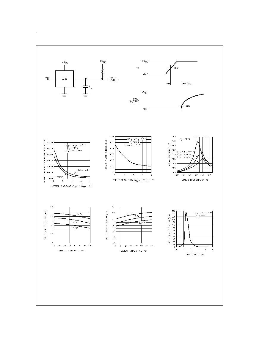
TRI-STATE Test Circuit and Waveforms
(Continued)
Typical Performance Characteristics
DS012811-4
DS012811-5
Offset and Fullscale
Error Change vs
Reference Voltage
DS012811-6
Linearity Error Change
vs Reference Voltage
DS012811-7
Mux ON Resistance
vs Input Voltage
DS012811-8
Digital Supply Current
vs Temperature
DS012811-9
Analog Supply Current
vs Temperature
DS012811-10
Current Consumption in
Standby Mode vs Voltage
on Digital Input Pins
DS012811-11
www.national.com
5