ADC12048
12-Bit Plus Sign 216 kHz 8-Channel Sampling
Analog-to-Digital Converter
General Description
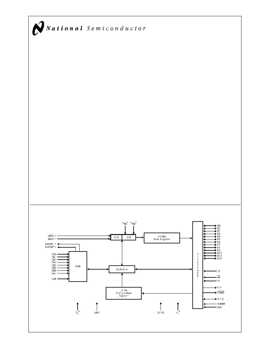
Operating from a single 5V power supply, the ADC12048 is a
12 bit + sign, parallel I/O, self-calibrating, sampling
analog-to-digital converter (ADC) with an eight input fully dif-
ferential analog multiplexer. The maximum sampling rate is
216 kHz.
On
request,
the
ADC
goes
through
a
self-calibration process that adjusts linearity, zero and
full-scale errors.
The ADC12048's 8-channel multiplexer is software program-
mable
to
operate
in
a
variety
of
combinations
of
single-ended, differential, or pseudo-differential modes. The
fully differential MUX and the 12-bit + sign ADC allows for the
difference between two signals to be digitized.
The ADC12048 can be configured to work with many popular
microprocessors/microcontrollers and DSPs including Na-
tional's HPC family, Intel386 and 8051, TMS320C25, Mo-
torola MC68HC11/16, Hitachi 64180 and Analog Devices
ADSP21xx.
For complementary voltage references see the LM4040,
LM4041 or LM9140.
Features
n
8-channel programmable Differential or Single-Ended
multiplexer
n
Programmable Acquisition Times and user-controllable
Throughput Rates
n
Programmable data bus width (8/13 bits)
n
Built-in Sample-and-Hold
n
Programmable Auto-Calibration and Auto-Zero cycles
n
Low power standby mode
n
No missing codes
Key Specifications
(f
CLK
= 12 MHz)
n
Resolution
12-bits + sign
n
13-bit conversion time
3.6 çs, max
n
13-bit throughput rate
216 ksamples/s, min
n
Integral Linearity Error (ILE)
Ý
1 LSB, max
n
Single Supply
+5V
Ý
10%
n
V
IN
Range
GND to V
A
+
n
Power consumption
-- Normal operation
34 mW, max
-- Stand-by mode
75 çw, max
Applications
n
Medical instrumentation
n
Process control systems
n
Test equipment
n
Data logging
n
Inertial guidance
Block Diagram
TRI-STATE
Û
is a registered trademark of National Semiconductor Corporation.
DS012387-1
April 2000
ADC12048
12-Bit
Plus
Sign
216
kHz
8-Channel
Sampling
Analog-to-Digital
Converter
ˋ 2000 National Semiconductor Corporation
DS012387
www.national.com
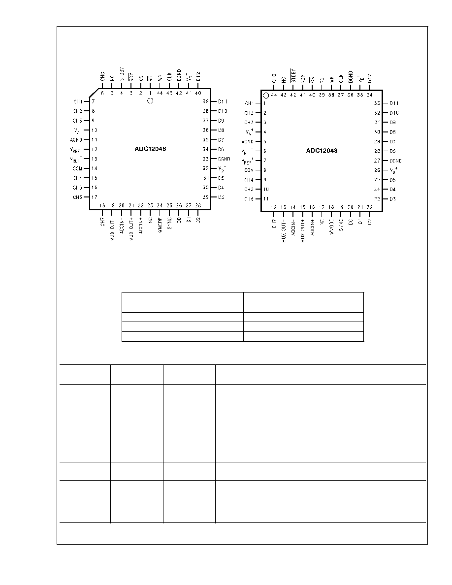
Connection Diagrams
Ordering Information
Industrial Temperature Range
Package
-40¯C
T
A
+85¯C
ADC12048CIV
PLCC
ADC12048CIVF
PQFP
ADC12048EVAL
Evaluation board
Pin Description
PLCC Pkg.
PQFP Pkg.
Pin Name
Description
Pin Number
Pin Number
6
44
CH0
The eight analog inputs to the Multiplexer. Active channels are selected
based on the contents of bits b3Ùb0 of the Configuration register. Refer
to section titled MUX for more details.
7
1
CH1
8
2
CH2
9
3
CH3
15
9
CH4
16
10
CH5
17
11
CH6
18
12
CH7
14
8
COM
This pin is another analog input pin used as a pseudo ground when the
multiplexer is configured in single-ended mode.
13
7
V
REF
+
Positive reference input. The operating voltage range for this input is
1V
V
REF
+
V
A
+ (see
Figure 3 and 4). This pin should be bypassed
to AGND at least with a parallel combination of a 10 çF and a 0.1 çF
(ceramic) capacitors. The capacitors should be placed as close to the
part as possible.
PLCC Package
DS012387-2
Order Number ADC12048CIV
See NS Package Number V44A
PQFP Package
DS012387-3
Order Number ADC12048CIVF
See NS Package Number VGZ44A
ADC12048
www.national.com
2

Pin Description
(Continued)
PLCC Pkg.
PQFP Pkg.
Pin Name
Description
Pin Number
Pin Number
12
6
V
REF
-
Negative reference input. The operating voltage range for this input is
0V
V
REF
-
V
REF
+ -1 (see
Figure 3 and 4). This pin should be
bypassed to AGND at least with a parallel combination of a 10 çF and
a 0.1 çF (ceramic) capacitor. The capacitors should be placed as close
to the part as possible.
19
13
MUX OUT-
The inverting (negative) and non-inverting (positive) outputs of the
multiplexer. The analog inputs to the MUX selected by bits b3Ùb0 of
the Configuration register appear at these pins.
21
15
MUX OUT+
20
14
ADCIN-
ADC inputs. The inverting (negative) and non-inverting (positive) inputs
into the ADC.
22
16
ADCIN+
24
18
WMODE
The logic state of this pin at power-up determines which edge of the
write signal (WR) will latch in data from the data bus. If tied low, the
ADC12048 will latch in data on the rising edge of the WR signal. If tied
to a logic high, data will he latched in on the falling edge of the WR
signal. The state of this pin should not be changed after power-up.
25
19
SYNC
The SYNC pin can be programmed as an input or an output. The
Configuration register's bit b8 controls the function of this pin. When
programmed as an input pin (b8 = 1), a rising edge on this pin causes
the ADC's sample-and-hold to hold the analog input signal and begin
conversion. When programmed as an output pin (b8 = 0), the SYNC
pin goes high when a conversion begins and returns low when
completed.
26Ù31
20Ù25
D0ÙD5
13-bit Data bus of the ADC12048. D12 is the most significant bit and
D0 is the least significant. The BW (bus width) bit of the Configuration
register (b12) selects between an 8-bit or 13-bit data bus width. When
the BW bit is cleared (BW = 0), D7ÙD0 are active and D12ÙD8 are
always in TRI-STATE. When the BW bit is set (BW = 1), D12ÙD0 are
active.
34Ù40
29Ù34
D6ÙD12
43
37
CLK
The clock input pin used to drive the ADC12048. The operating range
is 0.05 MHz to 12 MHz.
44
38
WR
WR is the active low WRITE control input pin. A logic low on this pin
and the CS will enable the input buffers of the data pins D12ÙD0. The
signal at this pin is used by the ADC12048 to latch in data on D12ÙD0.
The sense of the WMODE pin at power-up will determine which edge
of the WR signal the ADC12048 will latch in data. See WMODE pin
description.
1
39
RD
RD is the active low read control input pin. A logic low on this pin and
CS will enable the active output buffers to drive the data bus.
2
40
CS
CS is the active low Chip Select input pin. Used in conjunction with the
WR and RD signals to control the active data bus input/output buffers
of the data bus.
3
41
RDY
RDY is an active low output pin. The signal at this pin indicates when a
requested function has begun or ended. Refer to section Functional
Description and the digital timing diagrams for more detail.
4
42
STDBY
This is the standby active low output pin. This pin is low when the
ADC12048 is in the standby mode and high when the ADC12048 is out
of the standby mode or has been requested to leave the standby mode.
10
4
V
A
+
Analog supply input pin. The device operating supply voltage range is
+5V
Ý
10%. Accuracy is guaranteed only if the V
A
+ and V
D
+ are
connected to the same potential. This pin should be bypassed to AGND
with a parallel combination of a 10 çF and a 0.1 çF (ceramic) capacitor.
The capacitors should be placed as close to the supply pins of the part
as possible.
ADC12048
www.national.com
3

Pin Description
(Continued)
PLCC Pkg.
PQFP Pkg.
Pin Name
Description
Pin Number
Pin Number
11
5
AGND
Analog ground pin. This is the device's analog supply ground
connection. It should be connected through a low resistance and low
inductance ground return to the system power supply.
32 and 41
26 and 35
V
D
+
Digital supply input pins. The device operating supply voltage range is
+5V
Ý
10%. Accuracy is guaranteed only if the V
A
+ and V
D
+ are
connected to the same potential. This pin should be bypassed to
DGND with a parallel combination of a 10 çF and a 0.1 çF (ceramic)
capacitor. The capacitors should be placed as close to the supply pins
of the part as possible.
33 and 42
27 and 36
DGND
Digital ground pin. This is the device's digital supply ground connection.
It should be connected through a low resistance and low inductance
ground return to the system power supply.
ADC12048
www.national.com
4

Absolute Maximum Ratings
(Notes 1, 2)
If Military/Aerospace specified devices are required,
please contact the National Semiconductor Sales Office/
Distributors for availability and specifications.
Supply Voltage (V
A
+ and V
D
+)
6.0V
Voltage at all Inputs
-0.3V to V
+
+ 0.3V
|V
A
+ - V
D
+|
300 mV
|AGND - DGND|
300 mV
Input Current at Any Pin (Note 3)
Ý
30 mA
Package Input Current (Note 3)
Ý
120 mA
Power Dissipation (Note 4)
at T
A
= 25¯C
875 mW
Storage Temperature
-65¯C to +150¯C
Lead Temperature
VF Package
Vapor Phase (60 sec.)
210¯C
Infared (15 sec.)
220¯C
V Package, Infared (15 sec.)
300¯C
ESD Susceptibility (Note 5)
3.0 kV
Operating Ratings
(Notes 1, 2, 6, 7, 8, 9)
Temperature Range
(T
min
T
A
T
max
)
-40¯C
T
A
85¯C
Supply Voltage
V
A
+, V
D
+
4.5V to 5.5V
|V
A
+ - V
D
+|
100 mV
|AGND - DGND|
100 mV
V
IN
Voltage Range
at all Inputs
GND
V
IN
V
A
+
V
REF
+ Input Voltage
1V
V
REF
+
V
A
+
V
REF
- Input Voltage
0
V
REF
-
V
REF
+ - 1V
V
REF
+ - V
REF
-
1V
V
REF
V
A
+
V
REF
Common Mode
(Note 16)
0.1 V
A
+
V
REFCM
0.6 V
A
+
Converter DC Characteristics
The following specifications apply to the ADC12048 for V
A
+ = V
D
+ = 5V, V
REF
+ = 4.096V, V
REF
- = 0.0V, 12-bit + sign conver-
sion mode, f
CLK
= 12.0 MHz, R
S
= 25
, source impedance for V
REF
+ and V
REF
-
1
, fully differential input with fixed 2.048V
common-mode voltage (V
INCM
), and minimum acquisition time, unless otherwise specified. Boldface limits apply for T
A
= T
J
= T
MIN
to T
MAX
; all other limits T
A
= T
J
= 25¯C
Symbol
Parameter
Conditions
Typical
Limits
Unit
(Note 10)
(Note 11)
(Limit)
Resolution with No Missing
Codes
After Auto-Cal
13
Bits (max)
ILE
Integral Linearity Error
After Auto-Cal
(Notes 12, 17)
Ý
0.6
Ý
1
LSB (max)
DNL
Differential Non-Linearity
After Auto-Cal
Ý
1
LSB (max)
Zero Error
After Auto-Cal (Notes 13, 17)
V
INCM
= 5.0V
Ý
5.5
LSB (max)
V
INCM
= 2.048V
Ý
2.5
LSB (max)
V
INCM
= 0V
Ý
5.5
LSB (max)
Positive Full-Scale Error
After Auto-Cal (Notes 12, 17)
Ý
1.0
Ý
2.5
LSB (max)
Negative Full-Scale Error
After Auto-Cal (Notes 12, 17)
Ý
1.0
Ý
2.5
LSB (max)
DC Common Mode Error
After Auto-Cal (Note 14)
Ý
2
Ý
5.5
LSB (max)
TUE
Total Unadjusted Error
After Auto-Cal (Note 18)
Ý
1
LSB
Power Supply Characteristics
The following specifications apply to the ADC12048 for V
A
+ = V
D
+ = 5V, V
REF
+ = 4.096V, V
REF
- = 0.0V, 12-bit + sign conver-
sion mode, f
CLK
= 12.0 MHz, R
S
= 25
, source impedance for V
REF
+ and V
REF
-
1
, fully differential input with fixed 2.048V
common-mode voltage, and minimum acquisition time, unless otherwise specified. Boldface limits apply for T
A
= T
J
= T
MIN
to T
MAX
; all other limits T
A
= T
J
= 25¯C
Symbol
Parameter
Conditions
Typical
Limits
Unit
(Note 10)
(Note 11)
(Limit)
PSS
Power Supply Sensitivity
V
D
+ = V
A
+ = 5.0V
Ý
10% (Note 15)
Zero Error
V
REF
+ = 4.096V
Ý
0.1
LSB
Full-Scale Error
V
REF
- = 0V
Ý
0.5
LSB
Linearity Error
Ý
0.1
LSB
ADC12048
www.national.com
5