
ADC10461/ADC10462/ADC10464
10-Bit 600 ns A/D Converter with Input Multiplexer and
Sample/Hold
General Description
Using an innovative, patented multistep* conversion tech-
nique, the 10-bit ADC10461, ADC10462, and ADC10464
CMOS analog-to-digital converters offer sub-microsecond
conversion times yet dissipate a maximum of only 235 mW.
These converters perform 10-bit conversion in two lower-
resolution "flashes", yielding a fast A/D without the cost,
power consumption, and other problems associated with
true flash approaches. Dynamic performance (THD, S/N) is
guaranteed. The ADC10461 is pin-compatible with the
ADC1061 but is much faster, providing a convenient up-
grade path for the ADC1061.
The analog input voltage is sampled and held by an internal
sampling circuit. Input signals at frequencies from dc to over
200 kHz can, therefore, be digitized accurately without the
need for an external sample-and-hold circuit.
The ADC10462 and ADC10464 include a "speed-up" pin.
Connecting an external resistor between this pin and ground
reduces the typical conversion time to as little as 350 ns with
only a small increase in linearity error.
For ease of interface to microprocessors, the ADC10461,
ADC10462, and ADC10464 have been designed to appear
as a memory location or I/O port without the need for exter-
nal interface logic.
Features
n
Built-in sample-and-hold
n
Single +5V supply
n
1, 2, or 4-input multiplexer options
n
No external clock required
n
Speed adjust pin for faster conversions (ADC10462 and
ADC10464)
Key Specifications
n
Conversion Time
600 ns (typical)
n
Sampling Rate
800 kHz
n
Low Power Consumption
235 mW (max)
n
Total Harmonic Distortion (50 kHz)
-60 dB (max)
n
No Missing Codes
Over Temperature
Applications
n
Digital signal processor front ends
n
Instrumentation
n
Disk drives
n
Mobile telecommunications
Note: *U.S. Patent Number 4918449
Simplified Block Diagram
01110809
*ADC10461 Only
**ADC10462 and ADC10464 Only
***ADC10464 Only
November 2005
ADC10461/ADC10462/ADC10464
10-Bit
600
ns
A/D
Converter
with
Input
Multiplexer
and
Sample/Hold
� 2005 National Semiconductor Corporation
DS011108
www.national.com

Ordering Information
Industrial Temp Range
(-40�C
T
A
+85�C)
Channels
Package
ADC10461CIWM
1
M20B Small Outline
ADC10461CIWMX
1
M20B Small Outline Tape & Real
ADC10462CIWM
2
M24B Small Outline
ADC10462CIWMX
2
M24B Small Outline Tape & Real
ADC10464CIWM
4
M28B Small Outline
ADC10464CIWMX
4
M28B Small Outline Tape & Real
Connection Diagrams
01110810
Top View
01110811
Top View
01110812
Top View
ADC10461/ADC10462/ADC10464
www.national.com
2

Pin Descriptions
Pin Function
Description
DV
CC
, AV
CC
Digital and analog positive supply voltage inputs. Connect both to the same voltage source, but
bypass separately with a 0.1 �F ceramic capacitor in parallel with a 10 �F tantalum capacitor to
ground at each pin.
INT
Active low interrupt output. INT goes low at the end of each conversion, and returns high
following the rising edge of RD.
S/H
Sample/Hold control input. When this pin is forced low (and CS is low), the analog input signal is
sampled and a new conversion is initiated.
RD
Active low read control input. When this RD and CS are low, any data present in the output
registers will be placed onto the data bus.
CS
Active low Chip Select control input. When low, this pin enables the RD and S/H pins.
S0, S1
On the multiple-input devices (ADC10462 and ADC10464), these pins select the analog input
that will be connected to the A/D during the conversion. The input is selected based on the state
of S0 and S1 when S/H makes its High-to-Low transition (See the Timing Diagrams). The
ADC10464 includes both S0 and S1. The ADC10462 includes just S0, and the ADC10461 has
neither.
V
REF-
, V
REF+
Reference voltage inputs. They may be placed at any voltage between GND and V
CC
, but V
REF+
must be greater than V
REF-
. An input voltage equal to V
REF-
produces an output code of 0, and
an input voltage equal to (V
REF+
- 1 LSB) produces an output code of 1023.
V
IN
, V
IN0
, V
IN1
,
V
IN2
, V
IN3
Analog input pins. The ADC10461 has one input (V
IN
), the ADC10462 has two inputs (V
IN0
and
V
IN1
), and the ADC10464 has four inputs (V
IN0
, V
IN1
, V
IN2
and V
IN3
). The impedance of the input
source should be less than 500
for best accuracy and conversion speed. For accurate
conversions, no input pin (even one that is not selected) should be driven more than 50 mV
above V
CC
or 50 mV below ground.
GND, AGND,
DGND
Power supply ground pins. The ADC10461 has a single ground pin (GND), and the ADC10462
and ADC10464 have separate analog and digital ground pins (AGND and DGND) for separate
bypassing of the analog and digital supplies. The ground pins should be connected to a stable,
noise-free system ground. For the devices with two ground pins, both pins should be returned to
the same potential.
DB0�DB9
TRI-STATE
�
data output pins.
SPEED ADJ
(ADC10462 and ADC10464 only). This pin is normally left unconnected, but by connecting a
resistor between this pin and ground, the conversion time can be reduced. See the Typical
Performance Curves and the table of Electrical Characteristics.
ADC10461/ADC10462/ADC10464
www.national.com
3

Absolute Maximum Ratings
(Notes 1, 2)
If Military/Aerospace specified devices are required,
please contact the National Semiconductor Sales Office/
Distributors for availability and specifications.
Supply Voltage (V
+
= AV
CC
= DV
CC
)
-0.3V to +6V
Voltage at Any Input or Output
-0.3V to V
+
+ 0.3V
Input Current at Any Pin (Note 3)
5 mA
Package Input Current (Note 3)
20 mA
Power Consumption (Note 4)
875 mW
ESD Susceptibility (Note 5)
2000V
Soldering Information (Note 6)
N Package (10 Sec)
260�C
SO Package:
Vapor Phase (60 Sec)
215�C
Infrared (15 Sec)
220�C
Storage Temperature Range
-65�C to +150�C
Junction Temperature
150�C
Operating Ratings
(Notes 1, 2)
Temperature Range
T
MIN
T
A
T
MAX
ADC10461CIWM,
ADC10462CIWM,
ADC10464CIWM
-40�C
T
A
+85�C
Supply Voltage Range
4.5V to 5.5V
Package Thermal Resistance
Device
JA
(�C/W)
ADC10461CIWM
85
ADC10462CIWM
82
ADC10464CIWM
78
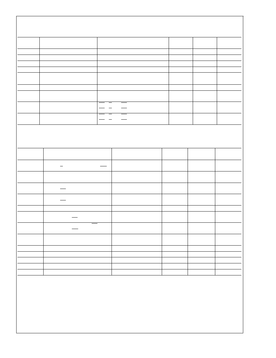
Converter Characteristics
The following specifications apply for V
+
= +5V, V
REF(+)
= +5V, V
REF(-)
= GND, and Speed Adjust pin unconnected unless oth-
erwise specified. Boldface limits apply for T
A
= T
J
= T
Min
to T
Max
; all other limits T
A
= T
J
= +25�C.
Symbol
Parameter
Conditions
Typical
(Note 7)
Limit
(Note 8)
Units
(Limit)
Resolution
10
Bits
Integral Linearity Error
R
SA
18 k
�
0.5
LSB
Offset Error
�
1.5
LSB (max)
Full-Scale Error
�
1
LSB (max)
Total Unadjusted Error
R
SA
18 k
�
0.5
LSB
Missing Codes
0
(max)
Power Supply Sensitivity
V
+
= 5V
�
5%, V
REF
= 4.5V
�
1/16
LSB
V
+
= 5V
�
10%, V
REF
= 4.5V
�
1
/
8
LSB
THD
Total Harmonic Distortion
f
IN
= 1 kHz, 4.85 V
P-P
f
IN
= 50 kHz, 4.85 V
P-P
f
IN
= 100 kHz, 4.85 V
P-P
f
IN
= 240 kHz, 4.85 V
P-P
-68
-66
-62
-58
-60
dB
dB (max)
dB
dB
SNR
Signal-to-Noise Ratio
f
IN
= 1 kHz, 4.
85 V
P-P
f
IN
= 50 kHz, 4.85 V
P-P
f
IN
= 100 kHz, 4.85 V
P-P
61
60
60
58
dB
dB (min)
dB
ENOB
Effective Number of Bits
f
IN
= 1 kHz, 4.85 V
P-P
f
IN
= 50 kHz, 4.85 V
P-P
9.6
9.5
9
Bits
Bits (min)
R
REF
Reference Resistance
650
400
(min)
R
REF
Reference Resistance
650
900
(max)
V
REF(+)
V
REF(+)
Input Voltage
V
+
+ 0.05
V (max)
V
REF(-)
V
REF(-)
Input Voltage
GND - 0.05
V (min)
V
REF(+)
V
REF(+)
Input Voltage
V
REF(-)
V (min)
V
REF(-)
V
REF(-)
Input Voltage
V
REF(+)
V (max)
V
IN
Input Voltage
V
+
+ 0.05
V (max)
V
IN
Input Voltage
GND - 0.05
V (min)
OFF Channel Input Leakage Current
CS = V
+
, V
IN
= V
+
0.01
3
�A (max)
ON Channel Input Leakage Current
CS = V
+
, V
IN
= V
+
�
1
-3
�A (max)
ADC10461/ADC10462/ADC10464
www.national.com
4
DC Electrical Characteristics
The following specifications apply for V
+
= +5V, V
REF(+)
= 5V V
REF(-)
= GND, and Speed Adjust pin unconnected unless other-
wise specified. Boldface limits apply for T
A
= T
J
= T
MIN
to T
MAX
; all other limits T
A
= T
J
= +25�C.
Symbol
Parameter
Conditions
Typical
(Note 7)
Limit (Note
8)
Units
(Limits)
V
IN(1)
Logical "1" Input Voltage
V
+
= 5.5V
2.0
V (min)
V
IN(0)
Logical "0" Input Voltage
V
+
= 4.5V
0.8
V (max)
I
IN(1)
Logical "1" Input Current
V
IN(1)
= 5V
0.005
3.0
�A (max)
I
IN(0)
Logical "0" Input Current
V
IN(0)
0V
-0.005
-3.0
�A (max)
V
OUT(1)
Logical "1" Output Voltage
V
+
= 4.5V, I
OUT
= -360 �A
2.4
V (min)
V
+
= 4.5V, I
OUT
= -10 �A
4.25
V (min)
V
OUT(0)
Logical "0" Output Voltage
V
+
= 4.5V, I
OUT
= 1.6 mA
0.4
V (max)
I
OUT
TRI-STATE Output Current
V
OUT
= 5V
V
OUT
= 0V
0.1
-0.1
50
-50
�A (max)
�A (max)
DI
CC
DV
CC
Supply Current
CS = S /H = RD = 0, R
SA
=
CS = S /H = RD = 0, R
SA
= 18 k
1.0
1.0
2
mA (max)
mA (max)
AI
CC
AV
CC
Supply Current
CS = S /H = RD = 0, R
SA
=
CS = S /H = RD = 0, R
SA
= 18 k
30
30
45
mA (max)
mA (max)
AC Electrical Characteristics
The following specifications apply for V
+
= +5V, t
r
= t
f
= 20 ns, V
REF(+)
= 5V, V
REF(-)
= GND, and Speed Adjust pin uncon-
nected unless otherwise specified. Boldface limits apply for T
A
= T
J
= T
MIN
to T
MAX
; all other limits T
A
= T
J
= +25�C.
Symbol
Parameter
Conditions
Typical
(Note 7)
Limit (Note
8)
Units
(Limits)
t
CONV
Mode 1 Conversion Time from Rising
Edge of S /H to Falling Edge of INT
CIN, CIWM Suffixes
R
SA
= 18k
600
375
750/900
ns (max)
ns
t
CRD
Mode 2 Conversion Time
CIN, CIWM Suffixes
Mode 2, R
SA
= 18k
850
530
1400
ns (max)
ns
t
ACC1
Access Time (Delay from Falling
Edge of RD to Output Valid)
Mode 1; C
L
= 100 pF
30
60
ns (max)
t
ACC2
Access Time (Delay from Falling
Edge of RD to Output Valid)
Mode 2; C
L
= 100 pF
900
t
CRD
+ 50
ns (max)
t
SH
Minimum Sample Time
(Figure 1) ; (Note 9)
250
ns (max)
t
1H
, t
0H
TRI-STATE Control (Delay from
Rising Edge of RD to High-Z State)
R
L
= 1k, C
L
= 10 pF
30
60
ns (max)
t
INTH
Delay from Rising Edge of RD to
Rising Edge of INT
C
L
= 100 pF
25
50
ns (max)
t
P
Delay from End of Conversion to
Next Conversion
50
ns (max)
t
MS
Multiplexer Control Setup Time
10
75
ns (max)
t
MH
Multiplexer Hold Time
10
40
ns (max)
C
VIN
Analog Input Capacitance
35
pF (max)
C
OUT
Logic Output Capacitance
5
pF (max)
C
IN
Logic Input Capacitance
5
pF (max)
Note 1: Absolute Maximum Ratings indicate limits beyond which damage to the device may occur. Operating Ratings indicate conditions for which the device is
functional. These ratings do not guarantee specific performance limits, however. For guaranteed specifications and test conditions, see the Electrical Characteristics.
The guaranteed specifications apply only for the test conditions listed. Some performance characteristics may degrade when the device is not operated under the
listed test conditions.
Note 2: All voltages are measured with respect to GND, unless otherwise specified.
Note 3: When the input voltage (V
IN
) at any pin exceeds the power supply rails (V
IN
<
GND or V
IN
>
V
+
) the absolute value of current at that pin should be limited
to 5 mA or less. The 20 mA package input current limits the number of pins that can safely exceed the power supplies with an input current of 5 mA to four.
Note 4: The maximum power dissipation must be derated at elevated temperatures and is dictated by T
JMAX
,
JA
and the ambient temperature, T
A
. The maximum
allowable power dissipation at any temperature is P
D
= (T
JMAX
- T
A
)/
JA
or the number given in the Absolute Maximum Ratings, whichever is lower. In most cases,
the maximum derated power dissipation will be reached only during fault conditions. For these devices, T
JMAX
for a board-mounted device can be in from the
Package Thermal Tables.
Note 5: Human body model, 100 pF discharged through a 1.5 k
resistor.
ADC10461/ADC10462/ADC10464
www.national.com
5