
ADC0831/ADC0832/ADC0834/ADC0838
8-Bit Serial I/O A/D Converters with Multiplexer Options
General Description
The ADC0831 series are 8-bit successive approximation A/D
converters with a serial I/O and configurable input multiplex-
ers with up to 8 channels. The serial I/O is configured to
comply with the NSC MICROWIRE
TM
serial data exchange
standard for easy interface to the COPS
TM
family of proces-
sors, and can interface with standard shift registers or µPs.
The 2-, 4- or 8-channel multiplexers are software configured
for single-ended or differential inputs as well as channel as-
signment.
The differential analog voltage input allows increasing the
common-mode rejection and offsetting the analog zero input
voltage value. In addition, the voltage reference input can be
adjusted to allow encoding any smaller analog voltage span
to the full 8 bits of resolution.
Features
n
NSC MICROWIRE compatible -- direct interface to
COPS family processors
n
Easy interface to all microprocessors, or operates
"stand-alone"
n
Operates ratiometrically or with 5 V
DC
voltage
reference
n
No zero or full-scale adjust required
n
2-, 4- or 8-channel multiplexer options with address logic
n
Shunt regulator allows operation with high voltage
supplies
n
0V to 5V input range with single 5V power supply
n
Remote operation with serial digital data link
n
TTL/MOS input/output compatible
n
0.3" standard width, 8-, 14- or 20-pin DIP package
n
20 Pin Molded Chip Carrier Package (ADC0838 only)
n
Surface-Mount Package
Key Specifications
n
Resolution
8 Bits
n
Total Unadjusted Error
±
1
/
2
LSB and
±
1 LSB
n
Single Supply
5 V
DC
n
Low Power
15 mW
n
Conversion Time
32 µs
Typical Application
TRI-STATE
®
is a registered trademark of National Semiconductor Corporation.
COPS
TM
and MICROWIRE
TM
are trademarks of National Semiconductor Corporation.
DS005583-1
August 1999
ADC0831/ADC0832/ADC0834/ADC0838
8-Bit
Serial
I/O
A/D
Converters
with
Multiplexer
Options
© 1999 National Semiconductor Corporation
DS005583
www.national.com
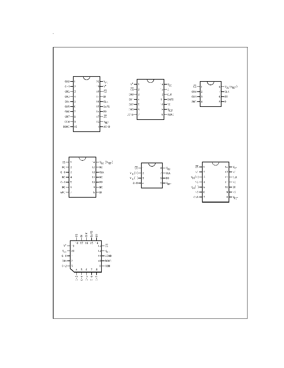
Connection Diagrams
ADC0838 8-Channel Mux
Small Outline/Dual-In-Line Package
(WM and N)
DS005583-8
Top View
ADC0834 4-Channel MUX
Small Outline/Dual-In-Line Package
(WM and N)
DS005583-30
COM internally connected to A GND
Top View
Top View
ADC0832 2-Channel MUX
Dual-In-Line Package (N)
DS005583-31
COM internally connected to GND.
V
REF
internally connected to V
CC
.
Top View
Top View
ADC0832 2-Channel MUX
Small Outline Package (WM)
DS005583-41
Top View
ADC0831 Single
Differential Input
Dual-In-Line Package (N)
DS005583-32
Top View
ADC0831 Single Differential Input
Small Outline Package (WM)
DS005583-42
Top View
ADC0838 8-Channel MUX
Molded Chip Carrier (PCC)
Package (V)
DS005583-33
www.national.com
2

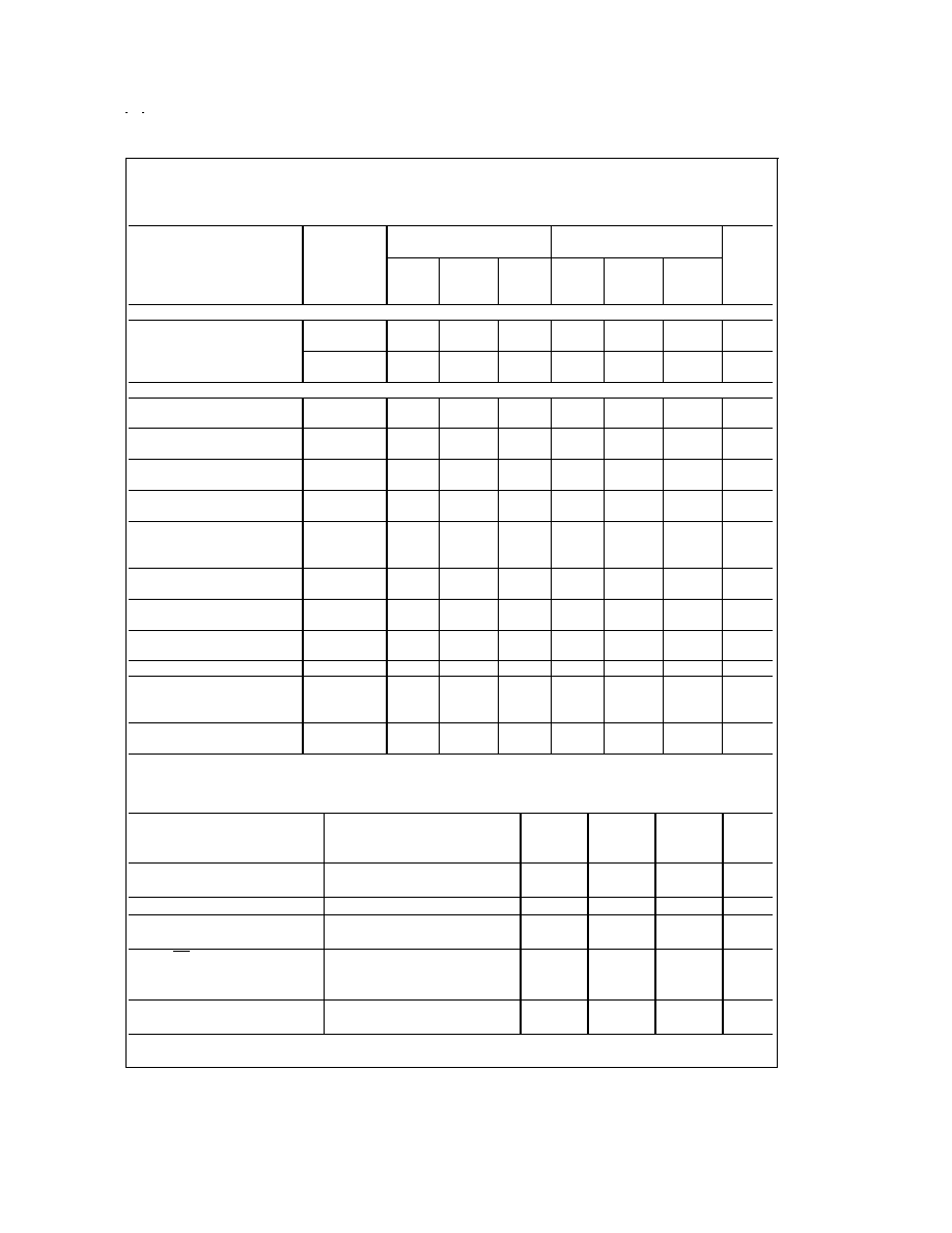
Ordering Information
Part Number
Analog Input
Total
Package
Temperature
Channels
Unadjusted Error
Range
ADC0831CCN
1
±
1
Molded (N)
0°C to +70°C
ADC0831CCWM
SO(M)
0°C to +70°C
ADC0832CIWM
2
±
1
SO(M)
-40°C to +85°C
ADC0832CCN
Molded (N)
0°C to +70°C
ADC0832CCWM
SO(M)
0°C to +70°C
ADC0834BCN
4
±
1
/
2
Molded (N)
0°C to +70°C
ADC0834CCN
±
1
Molded (N)
0°C to +70°C
ADC0834CCWM
SO(M)
0°C to +70°C
ADC0838BCV
8
±
1
/
2
PCC (V)
0°C to +70°C
ADC0838CCV
±
1
PCC (V)
0°C to +70°C
ADC0838CCN
Molded (N)
0°C to +70°C
ADC0838CIWM
SO(M)
-40°C to +85°C
ADC0838CCWM
SO(M)
0°C to +70°C
See NS Package Number M14B, M20B, N08E, N14A, N20A or V20A
www.national.com
3

Absolute Maximum Ratings
(Notes 1, 2)
If Military/Aerospace specified devices are required,
please contact the National Semiconductor Sales Office/
Distributors for availability and specifications.
Current into V
+
(Note 3)
15 mA
Supply Voltage, V
CC
(Note 3)
6.5V
Voltage
Logic Inputs
-0.3V to V
CC
+ 0.3V
Analog Inputs
-0.3V to V
CC
+ 0.3V
Input Current per Pin (Note 4)
±
5 mA
Package
±
20 mA
Storage Temperature
-65°C to +150°C
Package Dissipation
at T
A
=25°C (Board Mount)
0.8W
Lead Temperature (Soldering 10 sec.)
Dual-In-Line Package (Plastic)
260°C
Molded Chip Carrier Package
Vapor Phase (60 sec.)
215°C
Infrared (15 sec.)
220°C
ESD Susceptibility (Note 5)
2000V
Operating Ratings
(Notes 1, 2)
Supply Voltage, V
CC
4.5 V
DC
to 6.3 V
DC
Temperature Range
T
MIN
T
A
T
MAX
ADC0832/8CIWM
-40°C to +85°C
ADC0834BCN,
ADC0838BCV,
ADC0831/2/4/8CCN,
ADC0838CCV,
ADC0831/2/4/8CCWM
0°C to +70°C
Converter and Multiplexer Electrical Characteristics
The following specifications apply for
V
CC
= V+ = V
REF
= 5V, V
REF
V
CC
+0.1V, T
A
= T
j
= 25°C, and f
CLK
= 250 kHz unless otherwise specified. Boldface limits
apply from T
MIN
to T
MAX
.
Parameter
Conditions
CIWM Devices
BCV, CCV, CCWM, BCN
and CCN Devices
Typ
Tested
Design
Typ
Tested
Design
Units
(Note 12)
Limit
Limit
(Note 12)
Limit
Limit
(Note 13)
(Note 14)
(Note 13)
(Note 14)
CONVERTER AND MULTIPLEXER CHARACTERISTICS
Total Unadjusted Error
V
REF
=5.00 V
ADC0838BCV
(Note 6)
±
1
/
2
±
1
/
2
ADC0834BCN
±
1
/
2
±
1
/
2
LSB
(Max)
ADC0838CCV
±
1
±
1
ADC0831/2/4/8CCN
±
1
±
1
ADC0831/2/4/8CCWM
±
1
±
1
ADC0832/8CIWM
±
1
Minimum Reference
3.5
1.3
3.5
1.3
1.3
k
Input Resistance (Note 7)
Maximum Reference
3.5
5.9
3.5
5.4
5.9
k
Input Resistance (Note 7)
Maximum Common-Mode
Input Range (Note 8)
V
CC
+0.05
V
CC
+0.05
V
CC
+0.05
V
Minimum Common-Mode
Input Range (Note 8)
GND -0.05
GND -0.05
GND-0.05
V
DC Common-Mode Error
±
1/16
±
1
/
4
±
1/16
±
1
/
4
±
1
/
4
LSB
Change in zero
15 mA into V+
error from V
CC
=5V
V
CC
=N.C.
to internal zener
V
REF
=5V
operation (Note 3)
1
1
1
LSB
V
Z
, internal
MIN
15 mA into V+
6.3
6.3
6.3
diode breakdown
MAX
8.5
8.5
8.5
V
(at V
+
) (Note 3)
Power Supply Sensitivity
V
CC
=5V
±
5%
±
1/16
±
1
/
4
±
1
/
4
±
1/16
±
1
/
4
±
1
/
4
LSB
I
OFF
, Off Channel Leakage
On Channel=5V,
-0.2
-0.2
-1
µA
Current (Note 9)
Off Channel=0V
-1
On Channel=0V,
+0.2
+0.2
+1
µA
Off Channel=5V
+1
www.national.com
4
Converter and Multiplexer Electrical Characteristics
The following specifications apply for
V
CC
= V+ = V
REF
= 5V, V
REF
V
CC
+0.1V, T
A
= T
j
= 25°C, and f
CLK
= 250 kHz unless otherwise specified. Boldface limits
apply from T
MIN
to T
MAX
. (Continued)
Parameter
Conditions
CIWM Devices
BCV, CCV, CCWM, BCN
and CCN Devices
Typ
Tested
Design
Typ
Tested
Design
Units
(Note 12)
Limit
Limit
(Note 12)
Limit
Limit
(Note 13)
(Note 14)
(Note 13)
(Note 14)
CONVERTER AND MULTIPLEXER CHARACTERISTICS
I
ON
, On Channel Leakage
On Channel=0V,
-0.2
-0.2
-1
µA
Current (Note 9)
Off Channel=5V
-1
On Channel=5V,
+0.2
+0.2
+1
µA
Off Channel=0V
+1
DIGITAL AND DC CHARACTERISTICS
V
IN(1)
, Logical "1" Input
V
CC
=5.25V
2.0
2.0
2.0
V
Voltage (Min)
V
IN(0)
, Logical "0" Input
V
CC
=4.75V
0.8
0.8
0.8
V
Voltage (Max)
I
IN(1)
, Logical "1" Input
V
IN
=5.0V
0.005
1
0.005
1
1
µA
Current (Max)
I
IN(0)
, Logical "0" Input
V
IN
=0V
-0.005
-1
-0.005
-1
-1
µA
Current (Max)
V
OUT(1)
, Logical "1" Output
V
CC
=4.75V
Voltage (Min)
I
OUT
=-360 µA
2.4
2.4
2.4
V
I
OUT
=-10 µA
4.5
4.5
4.5
V
V
OUT(0)
, Logical "0" Output
V
CC
=4.75V
0.4
0.4
0.4
V
Voltage (Max)
I
OUT
=1.6 mA
I
OUT
, TRI-STATE Output
V
OUT
=0V
-0.1
-3
-0.1
-3
-3
µA
Current (Max)
V
OUT
=5V
0.1
3
0.1
+3
+3
µA
I
SOURCE
, Output Source
V
OUT
=0V
-14
-6.5
-14
-7.5
-6.5
mA
Current (Min)
I
SINK
, Output Sink Current (Min)
V
OUT
=V
CC
16
8.0
16
9.0
8.0
mA
I
CC
, Supply Current (Max)
ADC0831, ADC0834,
0.9
2.5
0.9
2.5
2.5
mA
ADC0838
ADC0832
Includes Ladder
2.3
6.5
2.3
6.5
6.5
mA
Current
AC Characteristics
The following specifications apply for V
CC
= 5V, t
r
= t
f
= 20 ns and 25°C unless otherwise specified.
Typ
Tested
Design
Limit
Parameter
Conditions
(Note 12)
Limit
Limit
Units
(Note 13)
(Note 14)
f
CLK
, Clock Frequency
Min
10
kHz
Max
400
kHz
t
C
, Conversion Time
Not including MUX Addressing Time
8
1/f
CLK
Clock Duty Cycle
Min
40
%
(Note 10)
Max
60
%
t
SET-UP
, CS Falling Edge or
250
ns
Data Input Valid to CLK
Rising Edge
t
HOLD
, Data Input Valid
90
ns
after CLK Rising Edge
www.national.com
5