54LCX245
Low Voltage Bidirectional Transceiver with 5V Tolerant
Inputs and Outputs
General Description
The LCX245 contains eight non-inverting bidirectional buff-
ers with TRI-STATE
TM
outputs and is intended for bus ori-
ented applications. The device is designed for low voltage
(3.3V) V
CC
applications with capability of interfacing to a 5V
signal environment. The T/R input determines the direction
of data flow through the device. The OE input disables both
the A and B ports by placing them in a high impedance state.
The LCX245 is fabricated with an advanced CMOS technol-
ogy to achieve high speed operation while maintaining
CMOS low power dissipation.
Features
n
5V tolerant inputs and outputs
n
9ns t
PD
max, 10ÁA I
CCQ
max
n
Power down high impedance inputs and outputs
n
Supports live insertion/withdrawal
n
2.0V¡3.6V V
CC
supply operation
n
▒
24 mA output drive
n
Implements patented noise/EMI reduction circuitry
n
Functionally compatible with the 54 series 245
n
ESD performance:
Human body model
>
2000V
Machine model
>
200V
n
Standard Microcircuit Drawing (SMD) 5962-97543
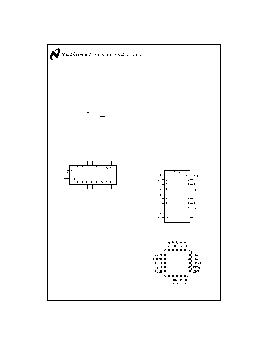
Logic Symbols
Pin Descriptions
Pin Names
Description
OE
Output Enable Input
T/R
Transmit/Receive Input
A
0
¡A
7
Side A Inputs or 3-STATE Outputs
B
0
¡B
7
Side B Inputs or 3-STATE Outputs
Connection Diagram
TRI-STATE
«
is a registered trademark of National Semiconductor Corporation.
DS101022-1
Pin Assignment
for DIP and Cerpack
DS101022-3
Pin Assignment
for LCC
DS101022-6
December 1998
54LCX245
Low
V
oltage
Bidirectional
T
ransceiver
with
5V
T
olerant
Inputs
and
Outputs
® 1998 National Semiconductor Corporation
DS101022
www.national.com
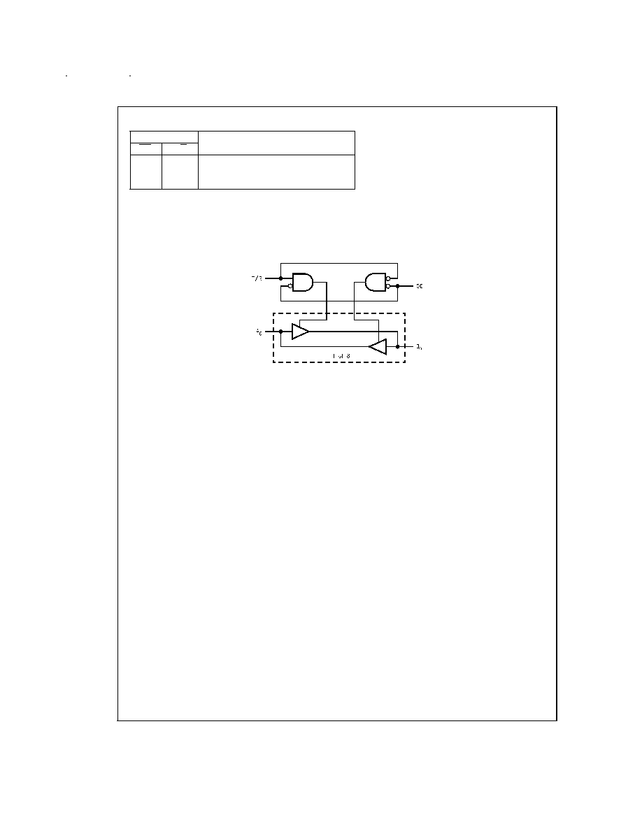
Truth Table
Inputs
Outputs
OE
T/R
L
L
Bus B
0
¡B
7
Data to Bus A
0
¡A
7
L
H
Bus A
0
¡A
7
Data to Bus B
0
¡B
7
H
X
HIGH Z State on A
0
¡A
7
, B
0
¡B
7
(Note 1)
H= High Voltage Level
L= Low Voltage Level
X= Immaterial
Z= High Impedance
Note 1: Unused bus terminals during HIGH Z State must be held HIGH or LOW.
Logic Diagram
DS101022-4
www.national.com
2
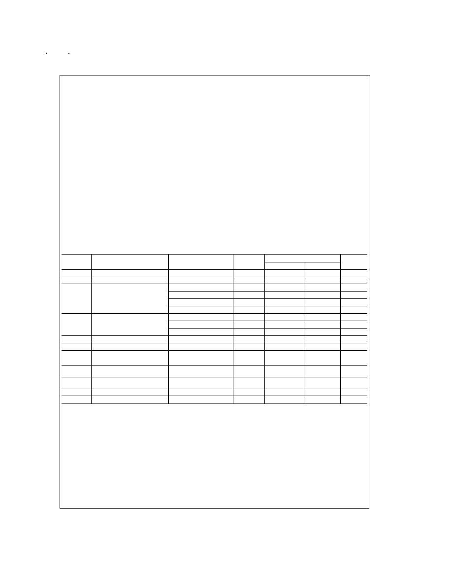
Absolute Maximum Ratings
(Note 2)
If Military/Aerospace specified devices are required,
please contact the National Semiconductor Sales Office/
Distributors for availability and specifications.
Supply Voltage (V
CC
)
-0.5V to +7.0V
DC Input Voltage (V
I
)
-0.5V to +7.0V
DC Input Diode Current (I
IK
)
V
I
<
GND
-50 mA
DC Output Diode Current (I
OK
)
V
O
<
GND
-50mA
V
O
V
CC
+50mA
DC Output Voltage (V
O
)
Output in High or Low State
-0.5V to V
CC
+ 0.5V
Output in TRI-STATE
-0.5V to 7.0V
DC Output Source or Sink Current
(I
O
)
▒
50mA
DC V
CC
or Ground Current
▒
200mA
Storage Temperature Range
(T
STG
)
-65░C to +150░C
Junction Temperature (T
J
)
CDIP
175░C
Recommended Operating
Conditions
(Note 3)
Supply Voltage (V
CC
)
Operating
2.0V to 3.6V
Data Retention
1.5V to 3.6V
Input Voltage (V
I
)
0V to 5.5V
Output Voltage (V
O
)
High or Low State
0V to V
CC
TRI-STATE
0V to 5.5V
Operating Temperature (T
A
)
54LCX
-55░C to +125░C
Minimum Input Edge Rate (
t/
V)
V
IN
from 0.8V to 2.0V, V
CC
= 3.0V
0ns/V to 10ns/V
Note 2: The Absolute Maximum Ratings are those values beyond which the
safety of the device cannot be guaranteed. The device should not be oper-
ated at these limits. The parametric values defined in the Electrical Charac-
teristics tables are not guaranteed at the Absolute Maximum Ratings. The
"Recommended Operating Conditions" table will define the conditions for ac-
tual device operation.
Note 3: I
O
Absolute Maximum Rating must be observed.
DC Electrical Characteristics
Symbol
Parameter
Conditions
V
CC
T
A
= -55░C to +125░C
Units
(V)
Min
Max
V
IH
HIGH Level Input Voltage
2.7¡3.6
2.0
V
V
IL
LOW Level Input Voltage
2.7¡3.6
0.8
V
V
OH
HIGH Level Output Voltage
I
OH
= -100 ÁA
2.7¡3.6
V
CC
- 0.2
V
I
OH
= -12 mA
2.7
2.2
V
I
OH
= -12 mA
3.0
2.4
V
I
OH
= -24 mA
3.0
2.2
V
V
OL
LOW Level Output Voltage
I
OL
= 100 ÁA
2.7¡3.6
0.2
V
I
OL
= 12 mA
2.7
0.4
V
I
OL
= 24 mA
3.0
0.55
V
I
I
Input Leakage Current
0
V
I
5.5V
2.7¡3.6
▒
5.0
ÁA
V
IKL
Clamp Diode Voltage
I
M
= -18mA
3.0
-1.2
V
I
OZ
TRI-STATE I/O Leakage
0
V
O
5.5V
2.7¡3.6
▒
5.0
ÁA
V
I
= V
IH
or V
IL
I
CCZ
Supply Current Outputs
TRI-STATE
V
I
= 5.5V or GND
2.7-3.6
10
ÁA
I
OFF
Power-Off Leakage Current
V
CC
= 0V, V
I
= 0V, V
M
=
5.5V
0
100
ÁA
I
CC
Quiescent Supply Current
V
I
= V
CC
or GND
2.7-3.6
10
ÁA
I
CC
Increase in I
CC
per Input
V
IH
= V
CC
-0.6V
2.7¡3.6
0.5
mA
www.national.com
3

AC Electrical Characteristics
Symbol
Parameter
T
A
= -55░C to +125░C, C
L
= 50pF, R
L
= 500
Units
V
CC
= 3.3V
▒
0.3V
V
CC
= 2.7V
Min
Max
Min
Max
t
PHL
Propagation Delay
1.5
8.0
1.5
9.0
ns
t
PLH
A
n
to B
n
or B
n
to A
n
1.5
8.0
1.5
9.0
t
PZL
Output Enable Time
1.5
10.0
1.5
11.0
ns
t
PZH
1.5
10.0
1.5
11.0
t
PLZ
Output Disable Time
1.5
8.0
1.5
9.0
ns
t
PHZ
1.5
8.0
1.5
9.0
t
OSHL
Output to Output Skew
1.0
1.0
ns
t
OSLH
(Notes 4, 5)
1.0
1.0
Note 4: Skew is defined as the absolute value of the difference between the actual propagation delay for any two separate outputs of the same device. The speci-
fication applies to any outputs switching in the same direction, either HIGH to LOW (t
OSHL
) or LOW to HIGH (t
OSLH
).
Note 5: Guaranteed but not tested (design characterization data).
Dynamic Switching Characteristics
Symbol
Parameter
Conditions
V
CC
(V)
T
A
= 25░C
Units
Max
V
OLP
Quiet Output Dynamic Peak V
OL
C
L
= 50 pF, V
IH
= 3.0V, V
IL
= 0V
3.0
1.0
V
V
OLV
Quiet Output Dynamic Valley V
OL
C
L
= 50 pF, V
IH
= 3.0V, V
IL
= 0V
3.0
-0.8
V
Capacitance
Symbol
Parameter
Conditions
Max
Units
C
IN
Input Capacitance
V
CC
= Open, V
I
= 0V or V
CC
10
pF
C
I/O
Input/Output Capacitance
V
CC
= 3.3V, V
I
= 0V or V
CC
12
pF
C
PD
Power Dissipation Capacitance
V
CC
= 3.3V, V
I
= 0V or V
CC
, f = 10 MHz
30
pF
www.national.com
4
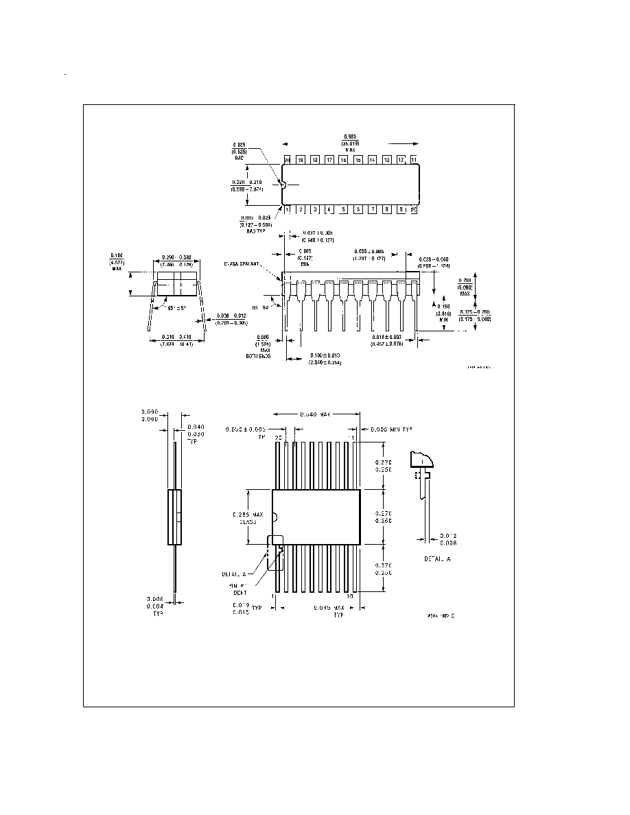
Physical Dimensions
inches (millimeters) unless otherwise noted
20-Lead Ceramic Dual-in-line
Package Number J20A
20-Lead Cerpack
Package Number W20A
www.national.com
5

Physical Dimensions
inches (millimeters) unless otherwise noted (Continued)
LIFE SUPPORT POLICY
NATIONAL'S PRODUCTS ARE NOT AUTHORIZED FOR USE AS CRITICAL COMPONENTS IN LIFE SUPPORT DE-
VICES OR SYSTEMS WITHOUT THE EXPRESS WRITTEN APPROVAL OF THE PRESIDENT OF NATIONAL SEMI-
CONDUCTOR CORPORATION. As used herein:
1. Life support devices or systems are devices or sys-
tems which, (a) are intended for surgical implant into
the body, or (b) support or sustain life, and whose fail-
ure to perform when properly used in accordance
with instructions for use provided in the labeling, can
be reasonably expected to result in a significant injury
to the user.
2. A critical component in any component of a life support
device or system whose failure to perform can be rea-
sonably expected to cause the failure of the life support
device or system, or to affect its safety or effectiveness.
National Semiconductor
Corporation
Americas
Tel: 1-800-272-9959
Fax: 1-800-737-7018
Email: support@nsc.com
www.national.com
National Semiconductor
Europe
Fax: +49 (0) 1 80-530 85 86
Email: europe.support@nsc.com
Deutsch Tel: +49 (0) 1 80-530 85 85
English
Tel: +49 (0) 1 80-532 78 32
Franþais Tel: +49 (0) 1 80-532 93 58
Italiano
Tel: +49 (0) 1 80-534 16 80
National Semiconductor
Asia Pacific Customer
Response Group
Tel: 65-2544466
Fax: 65-2504466
Email: sea.support@nsc.com
National Semiconductor
Japan Ltd.
Tel: 81-3-5639-7560
Fax: 81-3-5639-7507
20-Lead Leadless Chip Carrier
Package Number E20A
54LCX245
Low
V
oltage
Bidirectional
T
ransceiver
with
5V
T
olerant
Inputs
and
Outputs
National does not assume any responsibility for use of any circuitry described, no circuit patent licenses are implied and National reserves the right at any time without notice to change said circuitry and specifications.