54AC245
·
54ACT245
Octal Bidirectional Transceiver with TRI-STATE
®
Inputs/Outputs
General Description
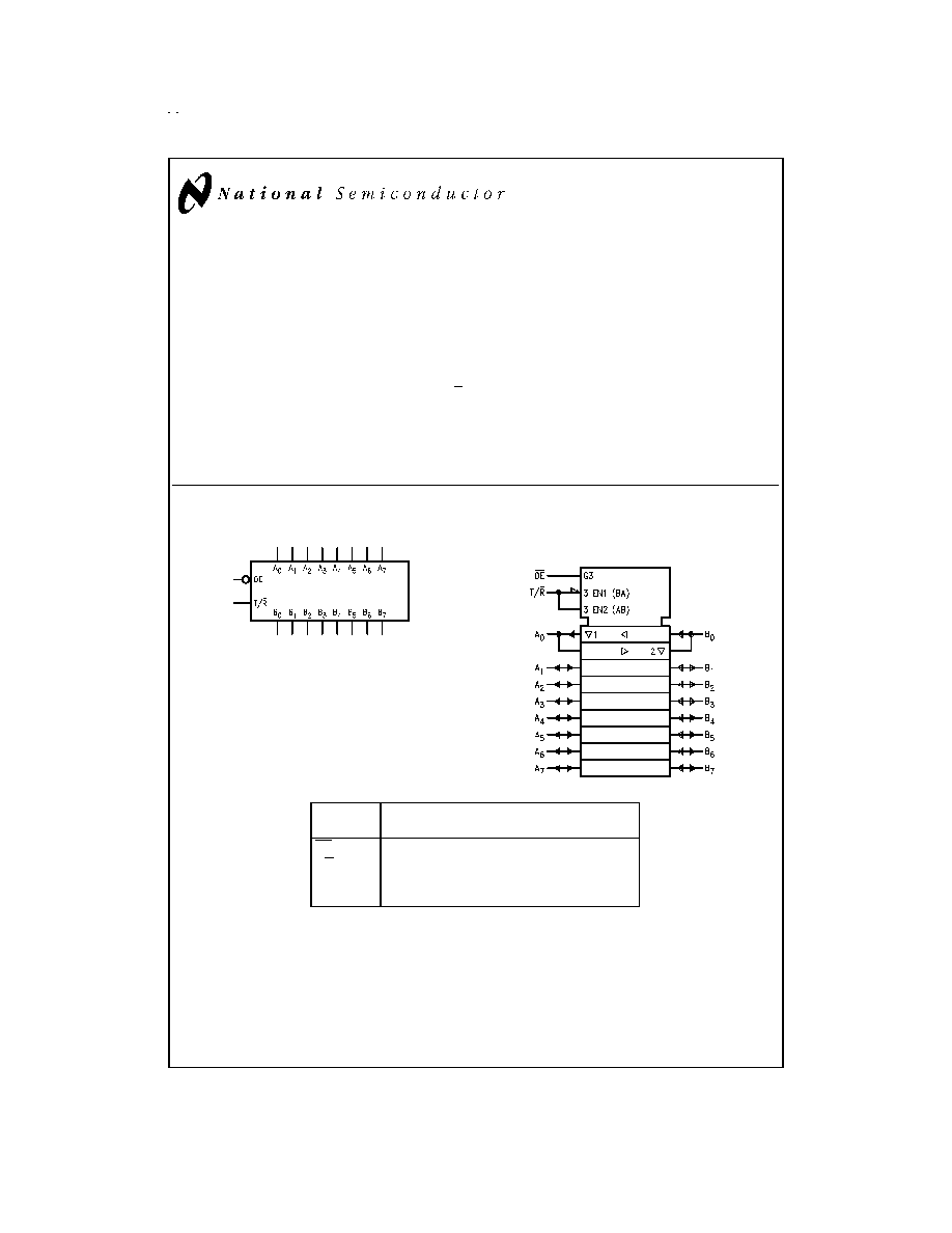
The 'AC/'ACT245 contains eight non-inverting bidirectional
buffers with TRI-STATE outputs and is intended for
bus-oriented applications. Current sinking capability is
24 mA at both the A and B ports. The Transmit/Receive (T/R)
input determines the direction of data flow through the bidi-
rectional transceiver. Transmit (active-HIGH) enables data
from A ports to B ports; Receive (active-LOW) enables data
from B ports to A ports. The Output Enable input, when
HIGH, disables both A and B ports by placing them in a HIGH
Z condition.
Features
n
I
CC
and I
OZ
reduced by 50%
n
Noninverting buffers
n
Bidirectional data path
n
A and B outputs source/sink 24 mA
n
'ACT245 has TTL-compatible inputs
n
Standard Microcircuit Drawing (SMD)
-- 'AC245: 5962-87758
-- 'ACT245: 5962-87663
Logic Symbols
Pin
Description
Names
OE
Output Enable Input
T/R
Transmit/Receive Input
A
0
A
7
Side A TRI-STATE Inputs or TRI-STATE Outputs
B
0
B
7
Side B TRI-STATE Inputs or TRI-STATE Outputs
TRI-STATE
®
is a registered trademark of National Semiconductor Corporation.
FACT
®
is a registered trademark of Fairchild Semiconductor Corporation.
DS100283-1
IEEE/IEC
DS100283-2
August 1998
54AC245
·
54ACT245
Octal
Bidirectional
T
ransceiver
with
TRI-ST
A
T
E
Inputs/Outputs
© 1998 National Semiconductor Corporation
DS100283
www.national.com

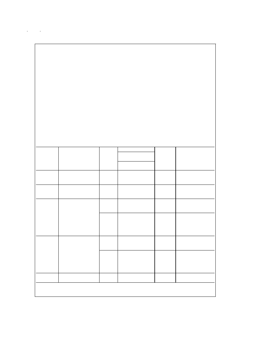
Connection Diagrams
Truth Table
Inputs
Outputs
OE
T/R
L
L
Bus B Data to Bus A
L
H
Bus A Data to Bus B
H
X
HIGH-Z State
H = HIGH Voltage Level
L = LOW Voltage Level
X = Immaterial
Pin Assignment for
DIP and Flatpak
DS100283-3
Pin Assignment for LCC
DS100283-4
www.national.com
2
Absolute Maximum Ratings
(Note 1)
If Military/Aerospace specified devices are required,
please contact the National Semiconductor Sales Office/
Distributors for availability and specifications.
Supply Voltage (V
CC
)
-0.5V to +7.0V
DC Input Diode Current (I
IK
)
V
I
= -0.5V
-20 mA
V
I
= V
CC
+ 0.5V
+20 mA
DC Input Voltage (V
I
)
-0.5V to V
CC
+ 0.5V
DC Output Diode Current (I
OK
)
V
O
= -0.5V
-20 mA
V
O
= V
CC
+ 0.5V
+20 mA
DC Output Voltage (V
O
)
-0.5V to V
CC
+ 0.5V
DC Output Source
or Sink Current (I
O
)
±
50 mA
DC V
CC
or Ground Current
per Output Pin (I
CC
or I
GND
)
±
50 mA
Storage Temperature (T
STG
)
-65°C to +150°C
Junction Temperature (T
J
)
CDIP
175°C
Recommended Operating
Conditions
Supply Voltage (V
CC
)
'AC
2.0V to 6.0V
'ACT
4.5V to 5.5V
Input Voltage (V
I
)
0V to V
CC
Output Voltage (V
O
)
0V to V
CC
Operating Temperature (T
A
)
54AC/ACT
-55°C to +125°C
Minimum Input Edge Rate (
V/
t)
'AC Devices
V
IN
from 30% to 70% of V
CC
V
CC
@
3.3V, 4.5V, 5.5V
125 mV/ns
Minimum Input Edge Rate (
V/
t)
'ACT Devices
V
IN
from 0.8V to 2.0V
V
CC
@
4.5V, 5.5V
125 mV/ns
Note 1: Absolute maximum ratings are those values beyond which damage
to the device may occur. The databook specifications should be met, without
exception, to ensure that the system design is reliable over its power supply,
temperature, and output/input loading variables. National does not recom-
mend operation of FACT
®
circuits outside databook specifications.
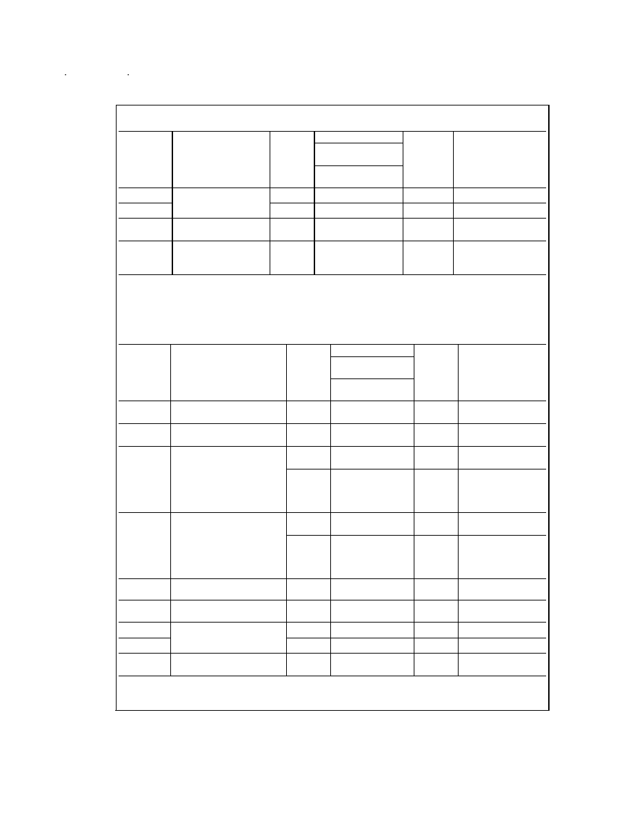
DC Characteristics for 'AC Family Devices
54AC
Symbol
Parameter
V
CC
T
A
=
Units
Conditions
(V)
-55°C to +125°C
Guaranteed
Limits
V
IH
Minimum High
3.0
2.1
V
OUT
= 0.1V
Level Input
4.5
3.15
V
or V
CC
- 0.1V
Voltage
5.5
3.85
V
IL
Maximum Low
3.0
0.9
V
OUT
= 0.1V
Level Input
4.5
1.35
V
or V
CC
- 0.1V
Voltage
5.5
1.65
V
OH
Minimum High
3.0
2.9
I
OUT
= -50 µA
Level Output
4.5
4.4
V
Voltage
5.5
5.4
(Note 2)
V
IN
= V
IL
or V
IH
3.0
2.4
-12 mA
4.5
3.7
V
I
OH
-24 mA
5.5
4.7
-24 mA
V
OL
Maximum Low
3.0
0.1
I
OUT
= 50 µA
Level Output
4.5
0.1
V
Voltage
5.5
0.1
(Note 2)
V
IN
= V
IL
or V
IH
3.0
0.50
12 mA
4.5
0.50
V
I
OL
24 mA
5.5
0.50
24 mA
I
IN
Maximum Input
5.5
±
1.0
µA
V
I
= V
CC
, GND
Leakage Current
www.national.com
3
DC Characteristics for 'AC Family Devices
(Continued)
54AC
Symbol
Parameter
V
CC
T
A
=
Units
Conditions
(V)
-55°C to +125°C
Guaranteed
Limits
I
OLD
(Note 3) Minimum
Dynamic Output
Current
5.5
50
mA
V
OLD
= 1.65V Max
I
OHD
5.5
-50
mA
V
OHD
= 3.85V Min
I
CC
Maximum Quiescent
5.5
80.0
µA
V
IN
= V
CC
Supply Current
or GND
I
OZT
Maximum I/O
V
I
(OE) = V
IL
, V
IH
Leakage Current
5.5
±
5.5
µA
V
I
= V
CC
, GND
V
O
= V
CC
, GND
Note 2: All outputs loaded; thresholds on input associated with output under test.
Note 3: Maximum test duration 2.0 ms, one output loaded at a time.
Note 4: I
IN
and I
CC
@
3.0V are guaranteed to be less than or equal to the respective limit
@
5.5V V
CC
.
I
CC
for 54AC
@
25°C is identical to 74AC
@
25°C.
DC Characteristics for 'ACT Family Devices
54ACT
Symbol
Parameter
V
CC
T
A
=
Units
Conditions
(V)
-55°C to +125°C
Guaranteed
Limits
V
IH
Minimum High Level
4.5
2.0
V
V
OUT
= 0.1V
Input Voltage
5.5
2.0
or V
CC
- 0.1V
V
IL
Maximum Low Level
4.5
0.8
V
V
OUT
= 0.1V
Input Voltage
5.5
0.8
or V
CC
- 0.1V
V
OH
Minimum High Level
4.5
4.4
V
I
OUT
= -50 µA
Output Voltage
5.5
5.4
(Note 5)
V
IN
= V
IL
or V
IH
4.5
3.70
V
I
OH
-24 mA
5.5
4.70
-24 mA
V
OL
Maximum Low Level
4.5
0.1
V
I
OUT
= 50 µA
Output Voltage
5.5
0.1
(Note 5)
V
IN
= V
IL
or V
IH
4.5
0.50
V
I
OL
24 mA
5.5
0.50
24 mA
I
IN
Maximum Input Leakage
Current
5.5
±
1.0
µA
V
I
= V
CC
, GND
I
CCT
Maximum
5.5
1.6
mA
V
I
= V
CC
- 2.1V
I
CC
/Input
I
OLD
(Note 6) Minimum
Dynamic Output
Current
5.5
50
mA
V
OLD
= 1.65V Max
I
OHD
5.5
-50
mA
V
OHD
= 3.85V Min
I
CC
Maximum Quiescent
5.5
80.0
µA
V
IN
= V
CC
Supply Current
or GND
www.national.com
4
DC Characteristics for 'ACT Family Devices
(Continued)
54ACT
Symbol
Parameter
V
CC
T
A
=
Units
Conditions
(V)
-55°C to +125°C
Guaranteed
Limits
I
OZT
Maximum I/O
V
I
(OE) = V
IL
, V
IH
Leakage Current
5.5
±
5.0
µA
V
I
= V
CC
, GND
V
O
= V
CC
, GND
Note 5: All outputs loaded; thresholds on input associated with output under test.
Note 6: Maximum test duration 2.0 ms, one output loaded at a time.
Note 7: I
CC
for 54ACT
@
25°C is identical to 74ACT
@
25°C.
AC Electrical Characteristics
54AC
V
CC
T
A
= -55°C
Fig.
Symbol
Parameter
(V)
to +125°C
Units
No.
(Note 8)
C
L
= 50 pF
Min
Max
t
PLH
Propagation Delay
3.3
1.0
11.5
ns
A
n
to B
n
or B
n
to A
n
5.0
1.0
8.5
t
PHL
Propagation Delay
3.3
1.0
10.0
ns
A
n
to B
n
or B
n
to A
n
5.0
1.0
7.5
t
PZH
Output Enable Time
3.3
1.0
13.5
ns
5.0
1.0
10.0
t
PZL
Output Enable Time
3.3
1.0
14.5
ns
5.0
1.0
10.5
t
PHZ
Output Disable Time
3.3
1.0
13.5
ns
5.0
1.0
10.5
t
PLZ
Output Disable Time
3.3
1.0
14.0
ns
5.0
1.0
10.5
Note 8: Voltage Range 3.3 is 3.3V
±
0.3V
Voltage Range 5.0 is 5.0V
±
0.5V
AC Electrical Characteristics
54ACT
V
CC
T
A
= -55°C
Symbol
Parameter
(V)
to +125°C
Units
(Note 9)
C
L
= 50 pF
Min
Max
t
PLH
Propagation Delay
5.0
1.0
9.0
ns
A
n
to B
n
or B
n
to A
n
t
PHL
Propagation Delay
5.0
1.0
10.0
ns
A
n
to B
n
or B
n
to A
n
t
PZH
Output Enable Time
5.0
1.0
12.0
ns
t
PZL
Output Enable Time
5.0
1.0
13.0
ns
t
PHZ
Output Disable Time
5.0
1.0
12.0
ns
t
PLZ
Output Disable Time
5.0
1.0
12.0
ns
Note 9: Voltage Range 5.0 is 5.0V
±
0.5V
www.national.com
5