NJL5902R
- 1 -
(0.85)
1.54
(0.5)
2.6
(0.6
2)
1.9
0.65
0.20 0.20
0.65
0.5
0.
5
0.25
0.2
5
0.65
0.5
0.5
0.2
5
0.25
0.2
5
0.65
(
1
.
16)
PT CENTER
LED CENTER
0.85
0.7 0.85
0.5
0.4
0.5
0.25
0.8
COBP PHOTO REFLECTOR
GENERAL DESCRIPTION
The NJL5902R is the compact surface mount type photo reflector in which Lead (Pb)-free reflow soldering permitted (260
Ḟ
C,
2times). The NJL5902R reduced to the operating dark current of 1/6 compared with our conventional products/NJL5901R, and
has realized the high S/N ratio in the combination of the high output LED and a high sensitivity Si photo-transistor.
FEATURES
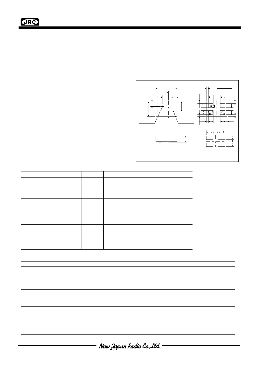
OUTLINE (typ.)
Unit : mm
Ṗ
Pb free solder re-flowing permitted: 260
Ḟ
C, 2times
Ṗ
Miniature, thin, surface mount: 1.9mm
Ṫ
2.6mm
Ṫ
0.8mm
Ṗ
Operating dark current: 0.3
ṁ
A max.
Ṗ
Built-in visible light cut-off filter
Ṗ
High output, high S/N ratio
APPLICATIONS
Ṗ
Detecting the location of optical pickup head for CD/DVD
Ṗ
Detecting the location of lens for DSC and Cellular phone's
camera module
Ṗ
Detecting the rotation of various motors
Ṗ
Paper edge detection and mechanism timing detection of
facsimile, copy machine etc.
ABSOLUTE MAXIMUM RATINGS
(Ta=25
Ḟ
C)
PARAMETER SYMBOL
RATINGS
UNIT
Emitter
Forward Current (Continuous)
Reverse Voltage (Continuous)
Power Dissipation
I
F
V
R
P
D
30
6
45
mA
V
mW
Detector
Collector-Emitter Voltage
Emitter-Collector Voltage
Collector Current
Collector Power Dissipation
V
CEO
V
ECO
I
C
P
C
16
6
10
25
V
V
mA
mW
Coupled
Total Power Dissipation
Operating Temperature
Storage Temperature
Reflow Soldering Temperature
P
tot
T
opr
T
stg
T
sol
60
-20
to
+85
-40
to
+85
260
mW
Ḟ
C
Ḟ
C
Ḟ
C
ELECTRO-OPTICAL CHARACTERISTICS
(Ta=25
Ḟ
C)
PARAMETER SYMBOL TEST
CONDITION
MIN
TYP
MAX
UNIT
Emitter
Forward Voltage
Reverse Current
Capacitance
V
F
I
R
C
t
I
F
=4mA
V
R
=6V
V
R
=0V,f=1MHz
--
--
--
--
--
25
1.4
10
--
V
ṁ
A
pF
Detector
Dark Current
Collector-Emitter Voltage
I
CEO
V
CEO
V
CE
=10V
I
C
=100
ṁ
A
--
16
--
--
0.2
--
ṁ
A
V
Coupled
Output Current
Operating Dark Current *1
Rise Time
Fall Time
I
O
I
CEOD
t
r
t
f
I
F
=4mA,V
CE
=2V,d=0.7mm
I
F
=4mA,V
CE
=2V
I
O
=100
ṁ
A,V
CE
=2V,RL=1K
,d=0.7mm
I
O
=100
ṁ
A,V
CE
=2V,RL=1K
,d=0.7mm
90
--
--
--
--
--
30
30
250
0.3
--
--
ṁ
A
ṁ
A
ṁ
s
ṁ
s
*1 Icoed may increase according to the periphery situation of the surface mounted product.
A:anode
K:cathode
C:collector
E:emitter
PCB pattern
NJL5902R
- 2 -
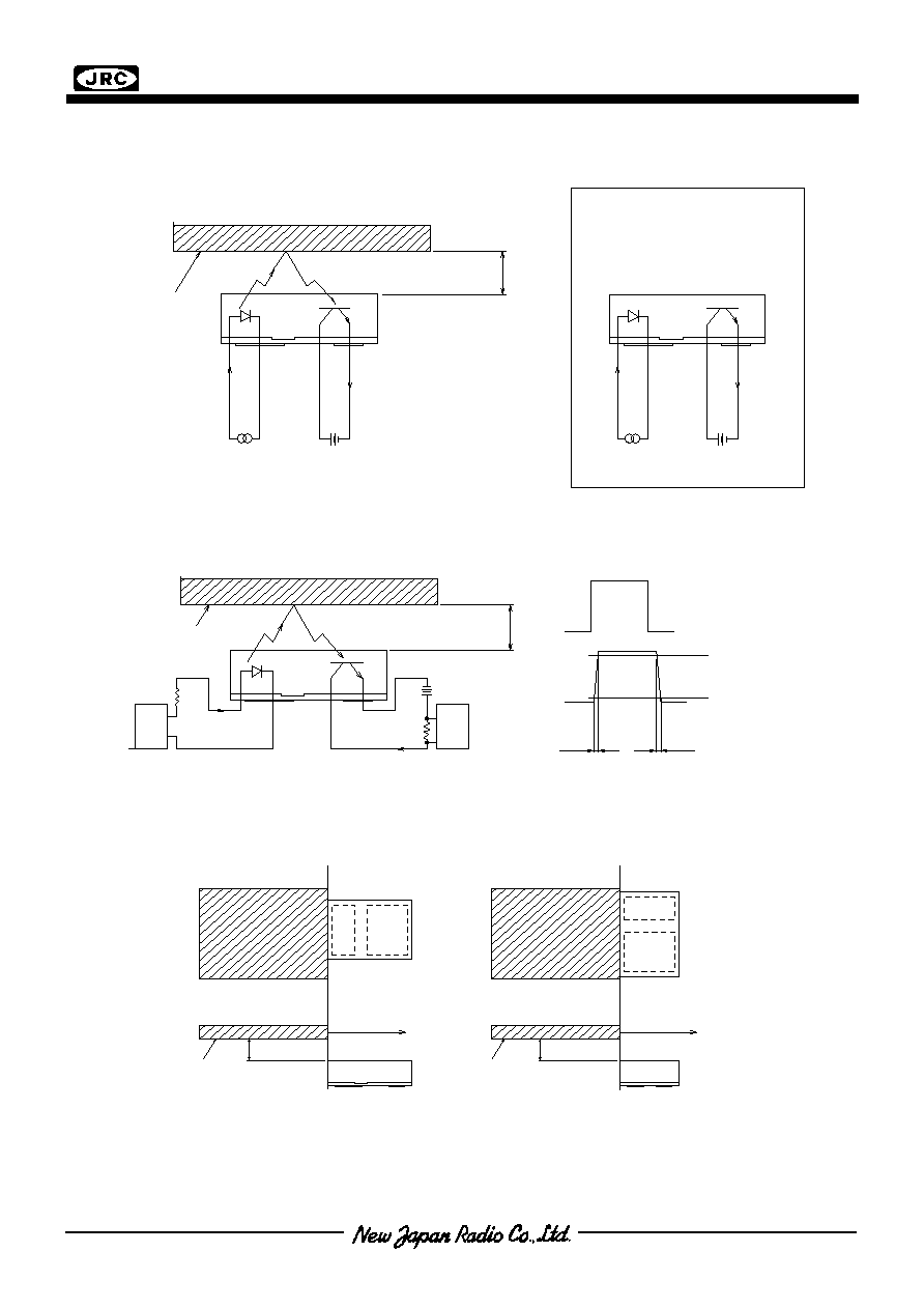
OUTPUT CURRENT TEST CONDITION
DARK CURRENT TEST CONDITION
The infrared signal from LED is reflected at the aluminum surface.
RESPONSE TIME TEST CONDITION
EDGE RESPONSE TEST CONDITION
0.7mm
Aluminum
Evapolation
Surface
I
F
I
CEOD
V
CE
I
F
I
CEOD
V
CE
0.7mm
I
F
Io
V+
R
L
R
D
P.G
OSC
Input
Output
tr
tf
10%
90%
Aluminum
Evapolation
Surface
l=0mm
0.7mm
0.7mm
l=0mm
Aluminum
Evaporation
Surface
Aluminum
Evaporation
Surface
Direction X
Direction Y
Light Sealed Dark Box
NJL5902R
- 3 -
Forward Voltage vs. Forward Current
1
10
100
0
1
2
Forward Voltage VF(V)
F
o
rw
ar
d C
u
r
r
e
n
t
I
F
(m
A
)
Forward Voltage vs. Temperature
0.8
1
1.2
1.4
1.6
-40
-20
0
20
40
60
80
100
Ambient Temperature Ta(
Ḟ
C)
F
o
r
w
a
r
d
V
o
l
t
age
V
F
(
V
)
Dark Current vs. Temperature
0.001
0.01
0.1
1
10
100
1000
10000
-40
-20
0
20
40
60
80
100
Ambient Temperature Ta(ḞC)
D
a
rk
Cu
rre
nt
I
c
e
o
(
n
A
)
Operating Dark Current vs. Temperature
0.01
0.1
1
10
-40
-20
0
20
40
60
80
100
Ambient Temperature Ta(ḞC)
O
per
at
i
n
g D
a
rk
C
u
r
r
ent
I
c
eod
(ṁ
A
)
Power Dissipation vs. Temperature
0
10
20
30
40
50
60
70
80
90
100
0
20
40
60
80
100
Ambient Temperature Ta(
Ḟ
C)
Power Dissipat
ion P(mW)
Forward Current vs. Temperature
0
5
10
15
20
25
30
35
40
45
50
0
20
40
60
80
100
Ambient Temperature Ta(ḞC)
Forward Current
I
F
(mA)
Total Power
Dissipation
Collector Power
Dissipation
TYPICAL CHARACTERISTICS
IF=4mA
IF=30mA
Vce=10V
IF=4mA,Vce=2V

NJL5902R
- 4 -
Output Current vs. Distance (Ta=25ḞC)
0
20
40
60
80
100
120
0
1
2
3
4
5
Reflector Distance d(mm)
R
e
l
a
t
i
v
e
O
u
t
put
C
u
r
r
ent
I
o
/
I
o(
m
a
x
.
)
(
%
)
Output Current vs. Edge Distance(Ta=25ḞC)
0
20
40
60
80
100
120
0
0.4
0.8
1.2
1.6
2
2.4
Edge Distance l(mm)
R
e
l
a
t
i
v
e
O
u
t
put
C
u
r
r
ent
I
o
/
I
o(
m
a
x
.
)
(
%
)
Output Current vs. Forward Current
(Ta=25
Ḟ
C)
0
50
100
150
200
250
300
350
400
450
500
0
2
4
6
8
10
Forward Current IF(mA)
O
u
tp
u
t
C
u
r
r
e
n
t
Io
(
ṁ
A
)
Output Current vs. Temperature
0
20
40
60
80
100
120
-40
-20
0
20
40
60
80
100
Ambient Temperature Ta(
Ḟ
C)
R
e
l
a
ti
ve
O
u
tp
u
t
C
u
r
r
e
n
t
Io
/I
o
(
2
5
Ḟ
C
)
(
%
)
Output Characteristics (Ta=25ḞC)
0
50
100
150
200
250
300
350
400
450
500
0
1
2
3
4
5
Collector-Emitter Voltage Vce(V)
O
u
tp
u
t
C
u
r
r
e
n
t
Io
(
ṁ
A
)
Vce Saturation (Ta=25ḞC)
0
0.1
0.2
0.3
0.4
0.5
0.1
1
10
Forward Current IF(mA)
C
o
l
l
e
c
t
o
r
-
Em
i
t
t
e
r
V
o
l
t
a
g
e
Vc
e
(
V)
IF=4mA,Vce=2V
IF=4mA,Vce=2V
IF=4mA,Vce=2V,d=0.7mm
Direction X
Direction Y
IVce=2V,d=0.7m
IF=4mA
IF=2mA
IF=6mA
IF=8mA
IF=10mA
Io=200
ṁ
A
Io=150
ṁ
A
Io=100
ṁ
A
Io=50
ṁ
A
NJL5902R
- 5 -
Spectral Response (Ta=25
Ḟ
C)
0
20
40
60
80
100
120
500
600
700
800
900
1000
Wavelength
(nm)
R
e
l
a
t
i
v
e
R
e
s
p
ons
e (
%
)
Switching Time vs. Load Resistance
(Ta=25
Ḟ
C)
1
10
100
1000
0.1
1
10
Load Resistance RL(k
)
S
w
it
c
h
in
g
T
i
m
e
t
(
ṁ
s
)
Vce=2V
td
tf
tr
Vce=2V,Io=100
ṁ
A
NJL5902R
- 6 -
PRECAUTION FOR HANDLING
1. Soldering to actual circuit board
Soldering condition
The surface temperature of plastic package is lower than 260
Ḟ
C.
Soldering Method
1) Reflow Method
Soldering to be done within twice under the recommended condition mentioned below
2) Reflow Method (In case of infrared heating)
The temperature profile is same as the above
Avoid direct irradiation to the plastic package because it may absorb the Infrared Radiation and its surface
temperature will be higher than the lead.
3) The other method
Avoid rapid heating up like dipping the devices directly into the melting solder or vapor phase method (VPS).
Solder the device in short time as soon as possible.
If the device is heated and kept in high temperature for longer time, its reliability would be affected.
2. Cleaning
Avoid washing the device after soldering by reflow method.
3. Attention in handling
1) Treat not to touch the lens surface.
2) Avoid dust and any other foreign materials on the lens surface such as paint, bonding material, etc.
4. Storage
Mount the device as soon as possible after opening the envelope. In order to prevent from degradation by the moisture at
the reflow process, the device is contained in damp proof packaging.
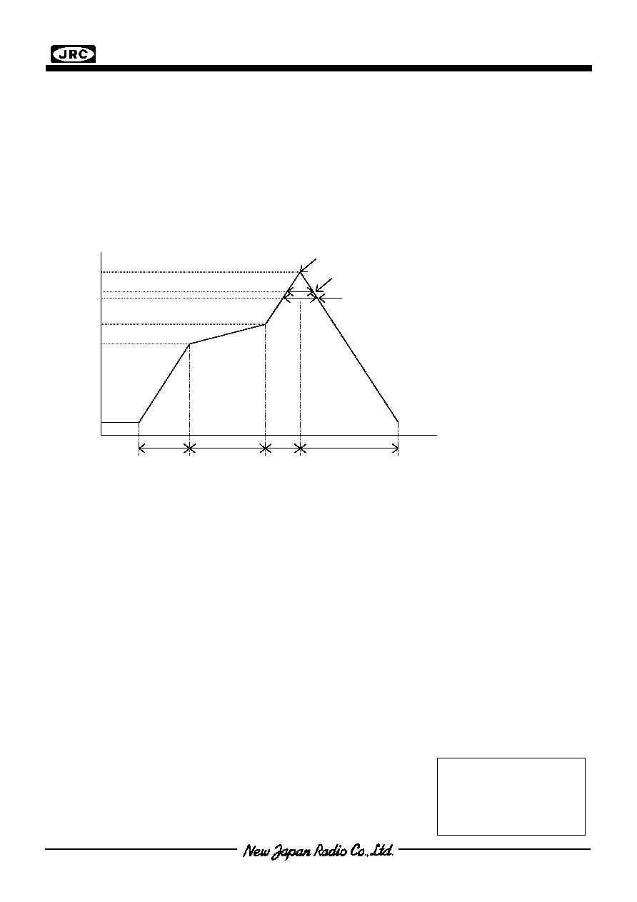
a b
c g
e
150
Ḟ
C
260
Ḟ
C
Room
Temp.
f
180
Ḟ
C
230
Ḟ
C
220
Ḟ
C
d
a : Temperature ramping rate : 1 to 4
Ḟ
C/s
b : Pre-heating temperature
time
: 150 to 180
Ḟ
C
: 60 to 120s
c : Temperature ramping rate : 1 to 4
Ḟ
C /s
d : 220
Ḟ
C or higher time
: Shorter than 60s
e : 230
Ḟ
C or higher time
: Shorter than 40s
f : Peak temperature
: Lower than 260
Ḟ
C
g : Temperature ramping rate : 1 to 6
Ḟ
C /s
The temperature of the surface of mold package
[CAUTION]
The specifications on this databook are only
given for information , without any guarantee
as regards either mistakes or omissions. The
application circuits in this databook are
described only to show representative usages
of the product and not intended for the
guarantee or permission of any right including
the industrial rights.