357 Beloit Street, P.O. Box 457, Burlington, WI 53105-0457 U.S.A. Phone 262/763-3591 FAX 262/763-2881
Email:
nelsales@nelfc.com
www.nelfc.com
HSTL
SD-A2C00 Series
PRELIMINARY
Description
The SD-A2C00 Series of quartz crystal oscillators provide HSTL compatible signals. Systems designers
may now specify space-saving, cost-effective packaged HSTL oscillators to meet their timing requirements.
Features
· Wide frequency range50.0MHz to 250.0MHz
· User specified tolerance available
· Will withstand vapor phase temperatures of 253°C
for 4 minutes maximum
· Space-saving alternative to discrete component
oscillators
· High shock resistance, to 1000g
· 3.3 volt operation
· Metal lid electrically connected to ground to
reduce EMI
· Fast rise and fall times <800 ps
· High Reliability - NEL HALT/HASS qualified for
crystal oscillator start-up conditions
· Low Jitter - Wavecrest jitter characterization
available
· Overtone technology
· High Q Crystal actively tuned oscillator circuit
· Power supply decoupling internal
· No internal PLL avoids cascading PLL problems
· High frequencies due to proprietary design
· Gold plated pads
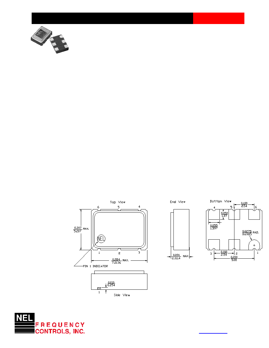
Electrical Connection
Pin Connection
1 V
CC
2 Enable/Disable
3 V
EE
4 Output
5 Output
Complement
6 V
CCO
CRYSTAL CLOCK OSCILLATORS
Data Sheet 0208D
Rev. B
357 Beloit Street, P.O. Box 457, Burlington, WI 53105-0457 U.S.A. Phone 262/763-3591 FAX 262/763-2881
Email:
nelsales@nelfc.com
www.nelfc.com
SD-A2C00 Series
Continued
HSTL
Operating Conditions and Output Characteristics
Electrical Characteristics
Parameter
Symbol
Conditions
Min
Typical
Max
Frequency
-----
-----
50.0MHz -----
250.0MHz
Duty Cycle
(2)
-----
@ V
O
/2
45/55% -----
55/45%
Logic 0
(2)
V
OL
-----
0.0V
-----
0.4V
Logic 1
(2)
V
OH
-----
1.0V
-----
1.2V
Rise & Fall Time
(2)
tr,tf
20-80%V
O
----- -----
800 psec
T
pd
(4)
-----
-----
-200 psec
-----
+200 psec
Jitter, RMS
(3)
-----
-----
-----
-----
3 psec
Enable (Low) voltage
-----
-----
-----
-----
800mV
Disable (High) voltage
-----
-----
2.00V
-----
-----
Frequency Stability
(1)
dF/F
Overall conditions including:
-100ppm
-----
+100ppm
voltage, calibration, temp.,
10 yr aging, shock, vibration
General Characteristics
Parameter
Symbol
Conditions
Min
Typical
Max
Supply Voltage
V
CC
-----
3.15V 3.3V
3.45V
Output Supply Current
V
CCO
----- 1.6V
-----
2.00V
Supply Current
I
CC
Ground Current
0.0 mA
-----
100 mA
Output current
I
O
Continuous Output Current
0.0 mA -----
±50.0 mA
Operating temperature
T
A
------
0°C -----
70°C
Storage temperature
T
S
----- -55°C -----
125°C
Power Dissipation
P
D
-----
-----
-----
345 mW
Lead temperature
T
L
Soldering, 10 sec. ----- -----
300°C
Start-up time
t
S
-----
-----
2 ms
10 ms
Environmental and Mechanical Characteristics
Mechanical Shock
Per MIL-STD-202, Method 213, Condition E
Thermal Shock
Per MIL-STD-833, Method 1011, Condition A
Vibration
0.060" double amplitude 10 Hz to 55 Hz, 35g's 55Hz to 2000 Hz
Soldering Condition
300°C for 10 seconds
Hermetic Seal
Leak rate less than 1 x 10
-8
atm.cc/sec of helium
Footnotes:
1) Standard frequency stability (±20,±25,±50ppm & others available)
2) Test Load per HSTL Class I of EIA/JEDEC Standard EIA/JESD8-6.
3) Jitter performance is frequency dependent. Please contact factory for full Wavecrest characterization.
4) Tpd is phse shift between the falling edge of pin 4 and the rising edge of pin 5.
5) Open to enable pin also enables the output.
Rev. B
CRYSTAL CLOCK OSCILLATORS
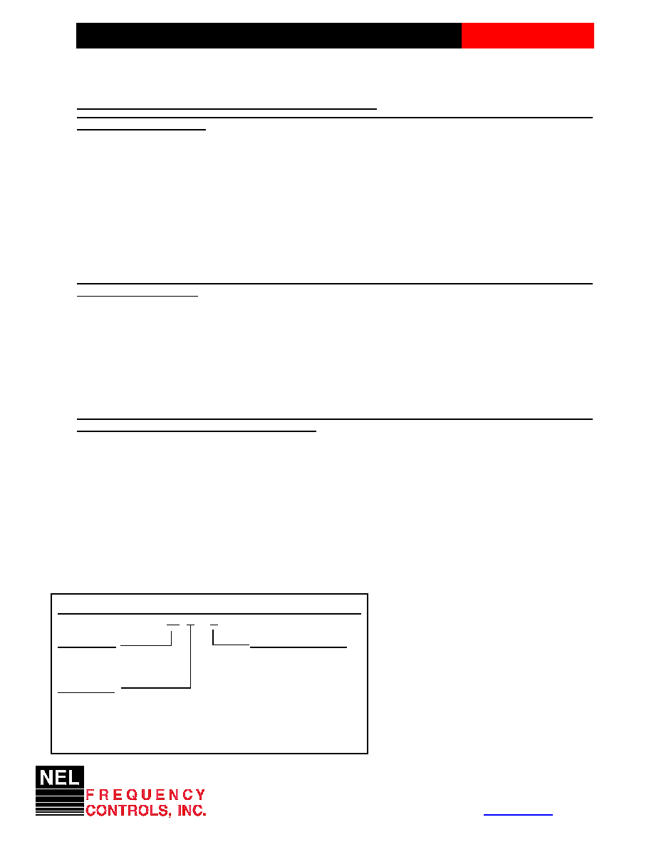
SD - A2C0X - FREQ
Package Code
Tolerance/Performance
SD 6 pad 5x7mm SMD
0 ±100ppm 0-70°C
1 ±50ppm 0-70°C
7 ±25ppm 0-70°C
Input Voltage
9 Customer Specific
Code Specification
A ±20ppm 0-70°C
A 3.3V
B ±50ppm -40 to +85°C
5V
C ±100ppm -40 to +85°C
Creating a Part Number
Data Sheet 0208D