
Preliminary Data Sheet
U13816EU2V0DS00
1
October 1998
Description
The V
RC
4171A
TM
is a companion chip to NEC's 64-bit V
R
41xx
TM
family of MIPS® RISC
microprocessors. Together, these two devices form the essential engine for most Windows®
CE-based handheld products.
Features
Y
Processor Interface
·
LCD module: *RD, *WR, *LCDCS and LCDRDY signals from the V
R
41xx
·
Other modules: mini-ISA-like 16-bit bus interface (as defined in the V
R
41xx)
·
256 x 18-bit on-chip color palette RAM for STN, DSTN, and TFT color panels
·
On-chip hardware cursor control (32 x 32 x 2)
Y
LCD Panel Support
·
240- and 480-line single scans
·
480-line dual scans
·
STN, DSTN, and TFT color panels
·
Nonindexed, true color (R, G, B): 15-bit (5-5-5) and 16-bit (5-6-5)
·
Controller functions (320 x 240, 480 x 240, 640 x 240, and 640 x 480)
Monochrome: up to 16 gray-scale levels (1, 2, or 4 bits/pixel)
Color depth: 1, 2, 4, 5, 6, 8, or 16 bits/pixel
Y
Frame Buffer Memory
·
One or two 3.3-volt 256K x 16-bit DRAMs (512K or 1 MB)
·
One 1 MB x 16-bit DRAM (2 MB)
Y
PC Card
TM
Slots (up to two)
·
PC Card or CompactFlash
TM
with adapter
·
PC Card or CompactFlash or Miniature Card
TM
PC Card controller: compliant with ExCA and PCMCIA release 2.1
CompactFlash controller: compliant with release 1.1
Miniature Card controller: compliant with release 1 (flash/ROM only)
Y
Other Features
·
Up to four general-purpose I/O (GPIO) pins
or up to two GPIO pins and two PCS pins
·
5-volt tolerance for LCD panel, frame buffer, and PC Card interface signals
·
208-pin LQFP package
·
3.3-volt ±5% operation
V
RC
4171A
Companion Chip for
V
R
4100 Family MIPS RISC Microprocessors
2
V
RC
4171A Companion Chip
Figure 1. Internal Block Diagram
mc_irq
reset_I
exca_memcs16_I
exca_iocs16_I
exca_iochrdy_I
spkrout
rio_I
smemwr_I
smemrd_I
siowr_I
siord_I
sbhe
reset_I
exca_memcs16_I
exca_iocs16_I
exca_iochrdy_I
smemwr_I
smemrd_I
siowr_I
siord_I
sbhe
98YL-0005B (7/98)
Slot A
PC Card
Control
(ExCA)
Slot B
PC Card
(ExCA)
or
Compact
Flash
Controls
Slot B
(Option)
Miniature
Card
Control
(Flash
ROM
Only)
LCD
Multifunction Pin Logic
A_ADR[25:12]
sd[15:0]
SD[15:0]
pc_addr_o[25:12]
SA[25:0]
sa[25:0]
sd[15:0]
sd[7:0]
pc/cf_addr[25:12]
mc_addr[24:12]
exca_reg_r_dat[7:0]
exca_reg_r_dat[7:0]
CLK
Divider
vclk
CFG
LOGIC
cfg_ctrl
lcdrdy
LCDRDY
IRQ
vplcdbl
vplcd
vpbias
vd_I[7:0]
vd_u[7:0]
tftd[17:16]
flm
loclk
dtmg
shclk
vwe_I
vcas_I_I
vcas_u_I
vras_I_I
vras_u_I
vma[8:0]
vd[15:0]
VPLCDBL
VPLCD
VPBIAS
VD_L[7:0]
VD_U[7:0]
TFTD[17:16]
FLM
LP
DTMG
SHCLK
*VWE
*VCAS[0]
*VCAS[1]
*VRAS[0]
*VRAS[1]
VMA[8:0]
VD[15:0]
pc_ce_I[2:1]
*A_CE[2:1]
pc_vppen1_o
A_VPPEN[1]
pc_vppen0_o
A_VPPEN[0]
pc_vccen1_I
*A_VCCEN[1]
pc_vccen0_I
*A_VCCEN[0]
pc_inpack_I
*A_INPACK
pc_reg_I_o
*A_REG
pc_crst_o
A_RESET
pc_wp_iocs16_I
A_WP
pc_rdy_busy_I
A_RDY/*A_BSY
pc_wait_I
*A_WAIT
pc_vs_i[2:1]
*A_VS[2:1]
pc_bvd_i[2:1]
A_BVD[2:1]
pc_cd_i[2:1]
*A_CD[2:1]
mc_vccen[1:0]
exca_int[5:3]
exca_int[7]
exca_int[12:9]
exca_int[15:14]
pc/cf_we_I
pc/cf_oe_I
pc/cf_ce_I_o[2:1]
pc_vppen1_o
pc_vppen0_o
pc/cf_vcc3_I_o
pc/cf_vcc5_I_o
pc_iord_I
pc_iowr_I
pc_we_I_o
pc_oe_I_o
pc_dir_o
pc_out_en_I
pc/cf_inpack_I
pc/cf_reg_I_o
pc/cf_crst_o
pc/cf_wp_iocs16_I
pc/cf_rdy_busy_I
pc/cf_wait_I
pc/cf_vs_i[2:1]
pc/cf_bvd_i[2:1]
pc/cf_cd_i[2:1]
pc/cf_dir_o
pc/cf_out_en_I
mc_oe_l
mc_we_I
mc_ceh_I
mc_cel_I
mc_dir_o
mc_crst_I
mc_rdy_busy_
mc_cd_I
mc_vs_i[2:1]
lcdcs_I
*LCDCS
clk8m
BUSCLK
GATED_I
rd_I
*RD
wr_I
*WR
X1
X2
MUX
MCLK
(V
RC
4171A)
MFP[35:0]
clk8m
spkrout
rio_I
reset_I
exca_memcs16_I
exca_iocs16_I
exca_iochrdy_I
smemwr_I
smemrd_I
siowr_I
siord_I
sbhe
exca_int[5:3]
exca_int[7]
exca_int[12:9]
exca_int[15:14]
clk8m
*SPKROUT
*RIO
*RESET
*MEMCS16
*IOCS16
IOCHRDY
*SMWR
*SMRD
*SIOWR
*SIORD
*SBHE
sa[25:0]
sd[7:0]
sa[25:0]
sa[23:0]
sd[15:0]
sa[11:0]
sd[15:0]
sa[23:0]
vmclk
3
V
RC
4171A Companion Chip
Figure 2. Pin Configuration
208-pin LQFP
(28 mm x 28 mm with 0.5 mm pin pitch)
Refer to the
V
RC
4171A Companion Chip User's Manual (document no. U13275EU1V0UM00) for
a detailed description of pin functions.
98YL-0004B (7/98)
2
1
3
4
5
6
7
8
9
10
11
12
13
14
15
16
17
18
19
20
21
22
23
24
25
26
27
28
29
30
31
32
33
34
35
36
37
38
39
40
41
42
43
44
45
46
47
48
49
50
51
52
GND
GND
*RESET
*A_CD[2]
*A_CD[1]
*A_VS[2]
*A_VS[1]
*A_VCCEN[1]
*A_VCCEN[0]
A_VPPEN[1]
A_VPPEN[0]
A_BVD[2]
A_BVD[1]
A_RESET
*SPKROUT
SA[0]
SA[1]
SA[2]
SA[3]
SA[9]
SA[10]
SA[11]
SA[4]
SA[5]
SA[6]
GND
VCC
SA[7]
SA[8]
SA[12]
SA[13]
SA[14]
SA[15]
SA[16]
SA[17]
SA[18]
SA[19]
SA[20]
SA[21]
SA[22]
SA[23]
*SMRD
*SMWR
*MEMCS16
*IOCS16
IOCHRDY
BUSCLK
*SBHE
*SIORD
*SIOWR
GND
GND
156
155
154
153
152
151
150
149
148
147
146
145
144
143
142
141
140
139
138
137
136
135
134
133
132
131
130
129
128
127
126
125
124
123
122
121
120
119
118
117
116
115
114
113
112
111
110
109
108
107
106
105
GND
GND
MFP[8]
MFP[7]
MFP[6]
MFP[5]
MFP[4]
MFP[3]
MFP[2]
MFP[1]
MFP[0]
NC
MCLK/NC
VPBIAS
VPLCDBL
VPLCD
VD_L[0]
VD_L[1]
VD_L[2]
VD_L[3]
VD_L[4]
VD_L[5]
VD_L[6]
VD_L[7]
GATED_I
GND
VCC
SHCLK
DTMG
LP
FLM
VD_U[0]
VD_U[1]
VD_U[2]
VD_U[3]
VD_U[4]
VD_U[5]
VD_U[6]
VD_U[7]
TFTD[16]
TFTD[17]
VD[0]
VD[8]
VD[1]
VD[9]
VD[2]
VD[10]
VD[3]
VD[11]
VD[4]
GND
GND
163
162
161
160
159
158
157
208
207
206
205
204
203
202
201
200
199
198
197
196
195
194
193
192
191
190
189
188
187
186
185
184
183
182
181
180
179
178
177
176
175
174
173
172
171
170
169
168
167
166
165
164
V
CC X2
X1
CRYL_INH
VD[12]
VD[5]
VD[13]
VD[6]
VD[14]
VD[7]
VD[15]
VMA[0]
VMA[1]
VMA[2]
VMA[3]
VMA[4]
VMA[5]
VMA[6]
VMA[7]
VMA[8]
*VWE
*VCAS[0]
*VCAS[1]
*VRAS[0]
*VRAS[1]
V
CC
GND
*RD
*WR
*LCDCS
LCDRDY
*RIO
SA[24]
SA[25]
IRQ
SD[15]
SD[14]
SD[13]
SD[12]
SD[11]
SD[10]
SD[9]
SD[8]
SD[7]
SD[6]
SD[5]
SD[4]
SD[3]
SD[2]
SD[1]
SD[0]
V
CC
56
57
58
53
54
55
59
60
61
62
63
64
65
66
67
68
69
70
71
72
73
74
75
76
77
78
79
80
81
82
83
84
85
86
87
88
89
90
91
92
93
94
95
96
97
98
99
100
101
102
103
104
V
CC
MFP[9]
MFP[10]
MFP[11]
MFP[12]
MFP[13]
MFP[14]
MFP[15]
MFP[16]
MFP[17]
MFP[18]
MFP[19]
MFP[20]
MFP[21]
MFP[22]
MFP[23]
MFP[24]
MFP[25]
MFP[26]
MFP[27]
MFP[28]
MFP[29]
MFP[30]
MFP[31]
MFP[32]
V
CC
GND
MFP[33]
MFP[34]
MFP[35]
A_ADR[12]
A_ADR[13]
A_ADR[14]
A_ADR[15]
A_ADR[16]
A_ADR[17]
A_ADR[18]
A_ADR[19]
A_ADR[20]
A_ADR[21]
A_ADR[22]
A_ADR[23]
A_ADR[24]
A_ADR[25]
A_RDY
*A_WAIT
*A_REG
A_WP
*A_INPACK
*A_CE[2]
*A_CE[1]
V
CC
V
RC
4171
4
V
RC
4171A Companion Chip
Caution:
Exposure to absolute maximum ratings for extended periods may affect device reliability;
exceeding the rating could cause permanent damage. Do not operate the device outside the
recommended operating conditions.
Note:
Values include package capacitance.
Table 1. Absolute Maximum Ratings
Parameter
Specification
Power supply voltage, V
DD
0.5 to +4.6 volts
Input voltage, V
I
3.3-volt input buffer (at V
I
< V
DD
+ 0.5 volt)
0.5 to +4.6 volts
3.3-volt fail-safe buffer (at V
I
< V
DD
+ 0.5 volt)
0.5 to +4.6 volts
5-volt tolerant (at V
I
< V
DD
+ 3.0 volts)
0.5 to +6.6 volts
Output voltage, V
O
3.3-volt output buffer (at V
O
< V
DD
+ 0.5 volt)
0.5 to +4.6 volts
5-volt tolerant buffer (at V
O
< V
DD
+ 3.0 volts)
0.5 to +6.6 volts
5-volt open-drain output buffer (at V
O
< V
DD
+ 3.0 volts)
0.5 to +6.6 volts
Latch-up current, I
LATCH
>1 A (typical)
Operating temperature, T
OPT
0 to +70°C
Storage temperature, T
STG
65 to +125°C
Table 2. Recommended Operating Conditions (
V
DD
= 3.3 V ±0.165 V: T
A
= 0 to +70°C)
3.3-Volt Interface Block
5-Volt Interface Block
Parameter
Symbol
Min.
Typ.
Max.
Min.
Max.
Unit
I/O power supply voltage
V
DD
3.135
3.3
3.465
V
Junction temperature
T
j
0
+100
0
+100
°C
High-level input voltage
V
IH
2.0
V
DD
2.0
5.5
V
Low-level input voltage
V
IL
0
0.8
0
0.8
V
Positive trigger voltage
V
P
1.50
2.70
2.20
2.55
V
Negative trigger voltage
V
N
0.60
1.4
0.84
1.01
V
Hysteresis voltage
V
H
1.10
1.5
1.10
1.5
V
Input rise/fall time
t
R
, t
F
0
200
0
200
ns
Input rise/fall time, Schmitt
t
R
, t
F
0
10
0
10
ns
I/O power supply voltage
V
DD
Table 3. Input/Output Capacitance (
V
DD
= V
I
= 0 V; f = 1 MHz)
Terminal
Symbol
Typ.
Max.
Unit
Input
C
IN
10
20
pF
Output
C
OUT
10
20
pF
I/O
C
I/O
10
20
pF

5
V
RC
4171A Companion Chip
.
Note:
Leave X1 open with no MCLK input.
Table 4. DC Characteristics (
V
DD
= 3.3 V ±0.165 V: T
j
= 0 to +70°C)
Parameter
Symbol
Min.
Typ.
Max.
Unit
Condition
All Buffer Types
Output current, low (3 mA)
I
OL
3
mA
V
OL
= 0.4 volt
Output current, low (6 mA)
I
OL
6
mA
V
OL
= 0.4 volt
5-Volt-Tolerant Block
Output current, high (3 mA)
I
OH
3
mA
V
OH
= 2.4 volts
Output current, high (6 mA)
I
OH
3
mA
V
OH
= 2.4 volts
3.3-Volt Interface Block
Output current, high (3 mA)
I
OH
3
mA
V
OH
= 2.4 volts
Output current, high (6 mA)
I
OH
6
mA
V
OH
= 2.4 volts
Output voltage, high
V
OH
0.9 V
DD
V
I
OH
= 500 µA
Output voltage, low
V
OL
0.1 V
DD
V
I
OL
= 1500 µA
V
CC
Current
LCD only
I
CC1
60
mA
V
CC
= 3.3 volts
MCLK = 60 MHz
VCLK = 20 MHz
PC Card off
65
mA
MCLK = 50 MHz
VCLK = 25 MHz
LCD plus PC Card active
I
CC2
90
mA
V
CC
= 3.3 volts
MCLK = 60 MHz
VCLK = 20 MHz
BUSCLK = 8 MHz
95
mA
MCLK = 50 MHz
VCLK = 25 MHz
Hibernate mode
I
CC3
100
µA
Gated_I enable
CRYL-INH enable
LCD panel off
Frame buffer PC Card
self-refresh off
Table 5. Clock Operation
Parameter
Symbol
Min.
Typ.
Max.
Unit
Condition
X1, X2 crystal input
f
xx
50
MHz
Crystal oscillator
X2 clock input
(Note)
F
x
66
MHz
External clock with 60 ns DRAMs
MCLK clock input
F
m
80
MHz
External clock with 50 ns DRAMs
66.6
MHz
External clock with 60 ns DRAMs
6
V
RC
4171A Companion Chip
Figure 3. Preliminary Uncharacterized AC Timing
98YL-0033B (4/98)
BUSCLK
*A_DBUFEN[2:1]
*SMRD, *SMWR,
*SIORD, *SIOWR
*MEMCS16, *IOCS16
IOCHRDY
Valid
Valid
Valid
Valid
Valid
Valid
Valid
*A_CE[2:1], *A_REG
*A_OE, *A_WE
*A_IOR, *A_IOW
SA[25:0], *SHBE
A_ADR[25:0]
SD[15:0] - Write
A_D[15:0] - Write
A_D[15:0] - Read
SD[15:0] - Read
A_DBUFDIR
t100
t3
t1
t2
t3
t1
t101
t115
t117
t116
t118
t103
t104
t106
t112
t113
t111
t110
t108
t107
t109
t102
t114
t105
7
V
RC
4171A Companion Chip
Note:
All values are subject to change without notice.
Table 6. Uncharacterized AC Characteristics
(refer to Figure 3)
Parameter
Symbol
Min.
Typ.
Max.
Unit
BUSCLK clock period
t
100
125
ns
Slot A Only
ns
*MEMCS16, *IOCS16
delay from SA[23:0] address and *SBHE valid
t
101
8
15
ns
*MEMCS16, *IOCS16
hold time from BUSCLK
t
102
3
4
ns
*A_CE[2:1], *A_REG
delay from SA[23:0] address and *SBHE valid
t
103
9
15
ns
A_ADR[25:0] address valid delay from SA[23:0] address and *SBHE valid
t
104
5
9
ns
IOCHRDY valid delay from *SMRD, *SMWR, *SIORD, *SIOWR
t
105
4
7
ns
IOCHRDY hold time from BUSCLK
t
106
4
7
ns
*A_OE, *A_WE
delay from *SMRD, *SMWR
t
107
6
10
ns
*A_IOR, *A_IOW
delay from *SIORD, *SIOWR
t
108
7
12
ns
*A_CE[2:1], *A_REG
delay from *SMRD, *SMWR, *SIORD, *SIOWR
t
109
9
15
ns
*A_OE, *A_WE
delay from *SMRD, *SMWR
t
110
6
10
ns
*A_IOR, *A_IOW
delay from *SIORD, *SIOWR
t
111
7
12
ns
SD[15:0] data valid to A_D[15:0] valid delay (write cycle)
t
112
13
17
ns
SD[15:0] data valid delay from A_D[15:0] valid (read cycle)
t
113
6
9
ns
SD[
15:0
] data hold time from *SMRD, *SMWR,*SIORD,*SIOWR
(
read cycle
)
t
114
4
6
9
ns
Slot A in Dual Slot Mode
ns
A_DBUFDIR delay from *SMRD, *SMWR, *SIORD, *SIOWR
t
115
6
9
ns
A_DBUFDIR hold time to *SMRD, *SMWR, *SIORD, *SIOWR
t
116
4
7
ns
A_DBUFEN[2:1] delay from *SMRD, *SMWR, *SIORD, *SIOWR
t
117
9
13
ns
A_DBUFEN[2:1] hold time to *SMRD, *SMWR, *SIORD, *SIOWR
t
118
5
8
ns

8
V
RC
4171A Companion Chip
Figure 4. DRAM Read Cycle
98YL-0034B (4/98)
MCLK
VMA [9:0]
Row
Col
Col
Col
Col
*VRAS
*VCAS
*VWE
VD [15:0]
tRP
Read
Data
Read
Data
Read
Data
Read
Data
tCAH
tRAS
tASC
tASR
tRAH
tCAS
tPC
tCAS
tCP
tCSH
tCRP
tRCD
T
tRAC

9
V
RC
4171A Companion Chip
Figure 5. DRAM Write Cycle
98YL-0035B (4/98)
MCLK
VMA [9:0]
Row
Col
Col
Col
Col
*VRAS
*VCAS
*VWE
VD [15:0]
Valid Data
Valid Data
Valid Data
Valid Data
tCAH
tRAS
tASC
tRAH
tCAS
tWCH
tCP
tCSH
tRCD
tWCS
T
tDH
tDS
tASR
10
V
RC
4171A Companion Chip
Note:
MCLK is from either XTAL on X1 and X2 or from the external oscillator.
Table 7. DRAM Read Cycle Characteristics
(refer to Figure 4)
Description
Symbol
Min.
Max.
Unit
Row address setup time
t
ASR
T ns
Row address hold time
t
RAH
T5 ns
Column address setup
t
ASC
T
ns
Column address hold time
t
CAH
T
ns
*VRAS pulse width
t
RAS
4.5T
ns
*VRAS precharge time
t
RP
3.5 T3
ns
*VRAS to *VCAS delay time
t
RCD
3.5 T + 2
ns
*VCAS hold time
t
CSH
3 T + 2
ns
*VCAS pulse width
t
CAS
T 1
ns
*VCAS precharge time
t
CP
T
ns
Data access time from *VRAS
t
RAC
4.5 T + 3
ns
Data access time from *VCAS
t
CAC
T + 3
ns
Table 8. DRAM Write Cycle Characteristics
(refer to Figure 5)
Description
Symbol
Min.
Max.
Unit
Row address setup time
t
ASR
T
ns
Row address hold time
t
RAH
T5
ns
Column address setup
t
ASC
T
ns
Column address hold time
t
CAH
T
ns
*VRAS pulse width
t
RAS
4.5 T
ns
*VRAS precharge time
t
RP
3.5 T3
ns
*VCAS to *VRAS precharge time
t
CRP
3 T
ns
*VCAS hold time
t
CSH
3 T+2
ns
*VCAS pulse width
t
CAS
T 1
ns
*VCAS precharge time
t
CP
T
ns
*VRAS to *VCAS delay time
t
RCD
3.5 T+2
ns
Write pulse setup time from *VCAS
t
WCS
2T
ns
Write pulse hold time from *VCAS
t
WCH
T
ns
Data setup time to *VCAS
t
DS
8
ns
Data hold time to *VCAS
t
DH
12
ns
11
V
RC
4171A Companion Chip
Figure 6. System Bus Cycle
Figure 7. VCAS Before VRAS Refresh Cycle
98YL-0036B (4/98)
X1
SD [15:0]
SA [23:0]
*LCDCS
*WR
*RD
LCDRDY
tWR
tRD
tLDH
Table 9. System Bus Cycle Characteristics
(refer to Figure 6)
Parameter
Symbol
Min
Max
Unit
LCDRDY to *LCDCS hold time
t
LDH
3
5
ns
*RD low to LCDRDY high time
t
RD
20
40
ns
*WR_L low to LCDRDY high time
t
WR
20
40
ns
98YL-0037B (4/98)
X1
*VRAS
*VCAS
tRP
tRAS
tCSR
Table 10. *VCAS Before *VRAS Refresh Characteristics
(refer to Figure 7)
Parameter
Symbol
Min
Max
Unit
*VCAS setup time
t
CSR
1.5 T2
ns
*VRAS pulse width
t
RAS
3.5 T
ns
*VRAS precharge time
t
RP
3.5 T2
ns
12
V
RC
4171A Companion Chip
Figure 8. Video Display Timing for TFT Panel
98YL-0062B (4/98)
FLM
DTMG
LP
LP
DTMG
SCK
13
V
RC
4171A Companion Chip
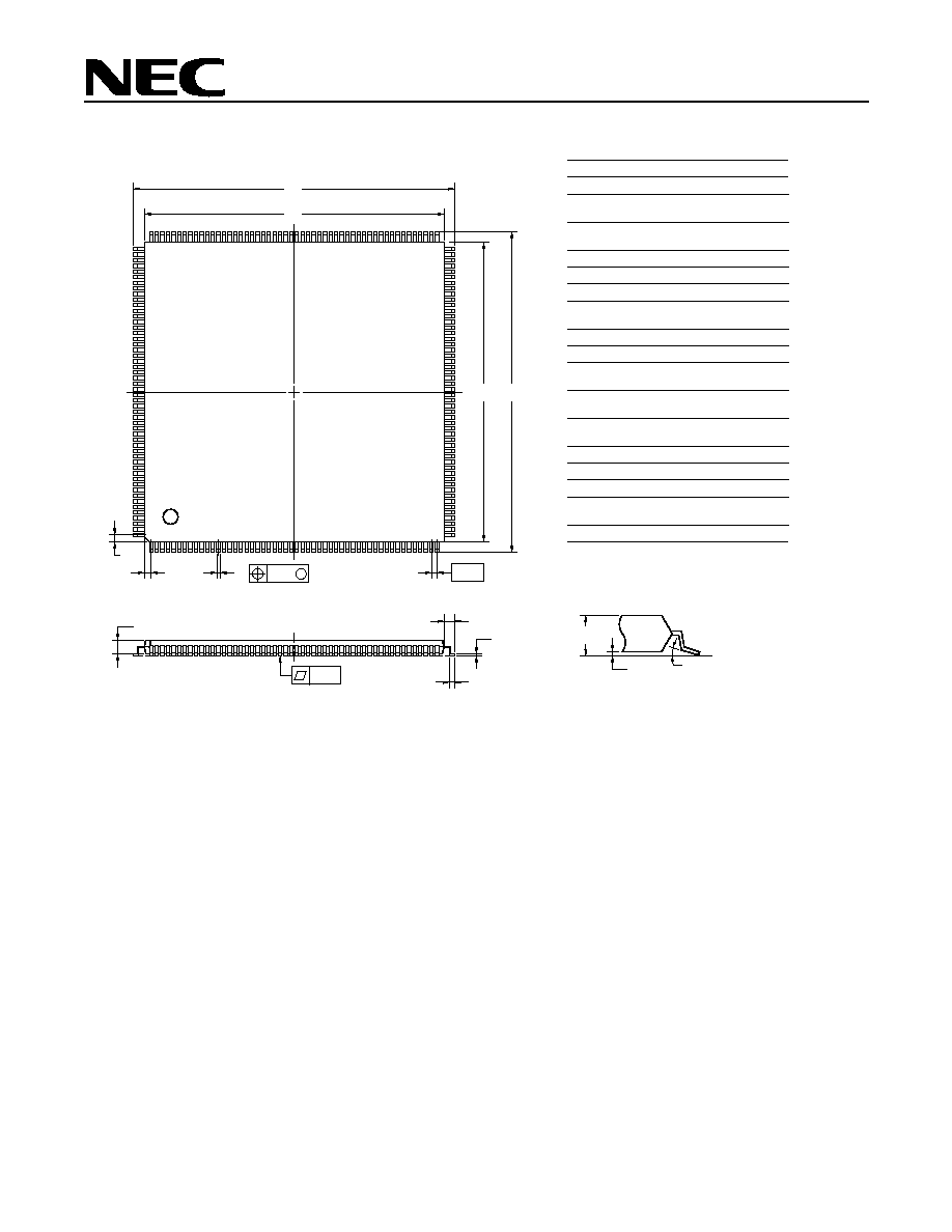
Figure 9. 208-Pin LQFP
NOTE
Each lead centerline is located within 0.10 mm (0.004 inch) of
its true position (T.P.) at maximum material condition.
ITEM
MILLIMETERS
INCHES
F
G
1.25
1.25
0.049
0.049
A
30.0
±
0.2
1.181
±
0.008
B
C
28.0
±
0.2
28.0
±
0.2
1.102
1.102
D
30.0
±
0.2
1.181
±
0.008
H
0.22
0.009
±
0.002
I
0.10
0.004
S
1.7 MAX.
0.067 MAX.
K
1.0
±
0.2
0.039
L
0.5
±
0.2
0.020+0.008
0.009
M
0.145
0.006
±
0.002
N
0.10
0.004
P
1.4
±
0.1
0.055
±
0.004
+0.05
0.04
J
0.5 (T.P.)
0.020 (T.P.)
S208GD-50-8EU-2
+0.055
0.045
J
H
I
G
N
L
K
detail of lead end
Q
0.125
±
0.075
0.005
±
0.003
+0.009
0.008
+0.009
0.008
R
3
°
3
°
+7
°
3
°
+7
°
3
°
+0.009
0.008
M
208
1
157
156
104
105
52
53
A
B
C
D
S
Q
R
F
M
P

14
V
RC
4171A Companion Chip

15
VRC4171A
Some of the information contained in this document may vary from country to country. Before using any NEC
product in your application, please contact a representative from the NEC office in your country to obtain a list of
authorized representatives and distributors who can verify the following:
Y
Device availability
Y
Ordering information
Y
Product release schedule
Y
Availability of related technical literature
Y
Development environment specifications (for example, specifications for third-party tools and components, host computers,
power plugs, AC supply voltages, and so forth)
Y
Network requirements
In addition, trademarks, export restrictions, and other legal issues may also vary from country to country.
NEC Electronics Inc. (U.S.)
Santa Clara, California
Tel: 800-366-9782
Fax: 800-729-9288
NEC Electronics (France) S.A.
Velizy-Villacoublay, France
Tel: 01-30-67 58 00
Fax: 01-30-67 58 99
NEC Electronics Hong Kong Ltd.
Seoul Branch
Seoul, Korea
Tel: 02-528-0303
Fax: 02-528-4411
NEC Electronics (Germany) GmbH
Duesseldorf, Germany
Tel: 0211-65 03 02
Fax: 0211-65 03 490
NEC Electronics (France) S.A.
Spain Office
Madrid, Spain
Tel: 01-504-2787
Fax: 01-504-2860
NEC Electronics Singapore Pte. Ltd.
United Square, Singapore 1130
Tel: 253-8311
Fax: 250-3583
NEC Electronics (UK) Ltd.
Milton Keynes, UK
Tel: 01908-691-133
Fax: 01908-670-290
NEC Electronics (Germany) GmbH
Scandinavia Office
Taeby, Sweden
Tel: 08-63 80 820
Fax: 08-63 80 388
NEC Electronics Taiwan Ltd.
Taipei, Taiwan
Tel: 02-719-2377
Fax: 02-719-5951
NEC Electronics Italiana s.r.l.
Milano, Italy
Tel: 02-66 75 41
Fax: 02-66 75 42 99
NEC Electronics Hong Kong Ltd.
Hong Kong
Tel: 2886-9318
Fax: 2886-9022/9044
NEC do Brasil S.A.
Sao Paulo-SP, Brasil
Tel: 011-889-1680
Fax: 011-889-1689
NEC Electronics (Germany) GmbH
Benelux Office
Eindhoven, the Netherlands
Tel: 040-2445845
Fax: 040-2444580

©1998 NEC Electronics Inc./Printed in U.S.A.
U13816EU2V0DS00
In North America: No part of this document may be copied or reproduced in any form or by any means without
the prior written consent of NEC Electronics Inc. (NECEL). The information in this document is subject to change
without notice. All devices sold by NECEL are covered by the provisions appearing in NECEL Terms and
Conditions of Sales only. Including the limitation of liability, warranty, and patent provisions. NECEL makes no
warranty, express, statutory, implied or by description, regarding information set forth herein or regarding the
freedom of the described devices from patent infringement. NECEL assumes no responsibility for any errors that
may appear in this document. NECEL makes no commitments to update or to keep current information
contained in this document. The devices listed in this document are not suitable for use in applications such as,
but not limited to, aircraft control systems, aerospace equipment, submarine cables, nuclear reactor control
systems, and life support systems. "Standard" quality grade devices are recommended for computers, office
equipment, communication equipment, test and measurement equipment, machine tools, industrial robots,
audio and visual equipment, and other consumer products. For automotive and transportation equipment, traffic
control systems, anti-disaster and anti-crime systems, it is recommended that the customer contact the
responsible NECEL salesperson to determine the reliability requirements for any such application and any cost
adder. NECEL does not recommend or approve use of any of its products in life support devices or systems or in
any application where failure could result in injury or death. If customers wish to use NECEL devices in
applications not intended by NECEL, customer must contact the responsible NECEL salespeople to determine
NECEL's willingness to support a given application.
For literature, call 1-800-366-9782 7 a.m. to 6 p.m. Pacific time
or FAX your request to 1-800-729-9288
or visit our web site at www.nec.com
NEC Electronics Inc.
CORPORATE HEADQUARTERS
2880 Scott Boulevard
Santa Clara, CA 95050-2554
TEL 408-588-6000
V
R
Series, V
RC
4171, V
RC
4171A, and V
R
4100 are either trademarks or registered trademarks of NEC Corporation
in the United States and/or other countries. MIPS is a registered trademark of MIPS Technology, Inc. PC Card
is a trademark of the Personal Computer Memory Card International Association. CompactFlash is a trademark
of the CompactFlash Association. Miniature Card is a trademark of the Miniature Card Implementers Forum.
Windows and Windows CE are either trademarks or registered trademarks of Microsoft Corporation.