Document Outline
- COVER
- DESCRIPTION
- FEATURES
- ORDERING INFORMATION
- SYSTEM CONFIGURATION EXAMPLE
- BLOCK DIAGRAM
- OUTLINE OF PINS
- PIN NAME
- PIN CONFIGURATION
- 1. PIN FUNCTIONS
- 1.1 PHY Layer Device Interface Signal
- 1.1.1 UTOPIA interface
- 1.1.2 PHY device control interface (external PHY mode, PHM of GMR register = 1)
- 1.2 Bus Interface Signals
- 1.2.1 Generic bus interface signals (PCI_MODE pin: low level)
- 1.2.2 PCI bus interface signal (PCI_MODE pin: high level)
- 1.3 Control Memory Interface Signals
- 1.4 PMD Interface Signals (internal PHY mode, PHM of GMR register = 0)
- 1.5 JTAG Boundary Scan Signals
- 1.6 Other Signals
- 1.7 Power and Ground
- 1.8 Pin Status during and after Reset
- 2. ELECTRICAL SPECIFICATIONS
- 3. PACKAGE DRAWING
- 4. RECOMMENDED SOLDERING CONDITIONS
The information in this document is subject to change without notice. Before using this document, please
confirm that this is the latest version.
Not all devices/types available in every country. Please check with local NEC representative for
availability and additional information.
MOS INTEGRATED CIRCUIT
Á
Á
Á
Á
PD98405
155M ATM INTEGRATED SAR CONTROLLER
Document No. S12689EJ2V0DS00 (2nd edition)
Date Published April 1999 N CP(K)
Printed in Japan
DATA SHEET
1997, 1999
®
The mark
shows major revised points.
DESCRIPTION
The
Á
PD98405 (NEASCOT-S20
TM
) is a high-performance SAR chip that performs segmentation and reassembly of
ATM cells. It has a PCI bus interface, a SONET/SDH 155-Mbps framer, and a clock recovery circuit and supports an
ABR function in hardware. The
Á
PD98405 conforms to ATM Forum and has the functions of the AAL-5 SAR
sublayer, ATM layer, and TC sublayer.
FEATURES
À
Conforms to ATM Forum.
À
Host bus interface supporting PCI bus/generic bus.
-
PCI interface (5/3.3 V, 32/64 bits, 33 MHz): Conforms to PCI Specification 2.1
-
Generic bus interface (5/3.3 V, 32 bits, 33 MHz)
À
AAL-5 SAR sublayer, ATM layer, and TC sublayer functions
À
Hardware support of AAL-5 processing
À
Software support of non-AAL-5 traffic
À
SONET STS-3c/SDH STM-1 155-Mbps framer function
À
Clock recovery/clock synthesizer function
À
Supports up to 32 K virtual channels (VCs)
À
Sixteen traffic shapers for VBR for transmission scheduling
À
Hardware support of CBR/VBR/ABR/UBR service
À
Supports multi-cell burst transfer for transmission and reception
À
MIB counter function
À
Supports LAN emulation function
À
Receive FIFO of 96 cells
À
External PHY devices connectable: UTOPIA Level-1 interface
À
0.35-
Á
m CMOS process, +5-/3.3-V power supply
-
Bus interface +5 V: +5-/3.3-V power supply
-
Bus interface +3.3 V: +3.3-V power supply
À
304-pin plastic QFP
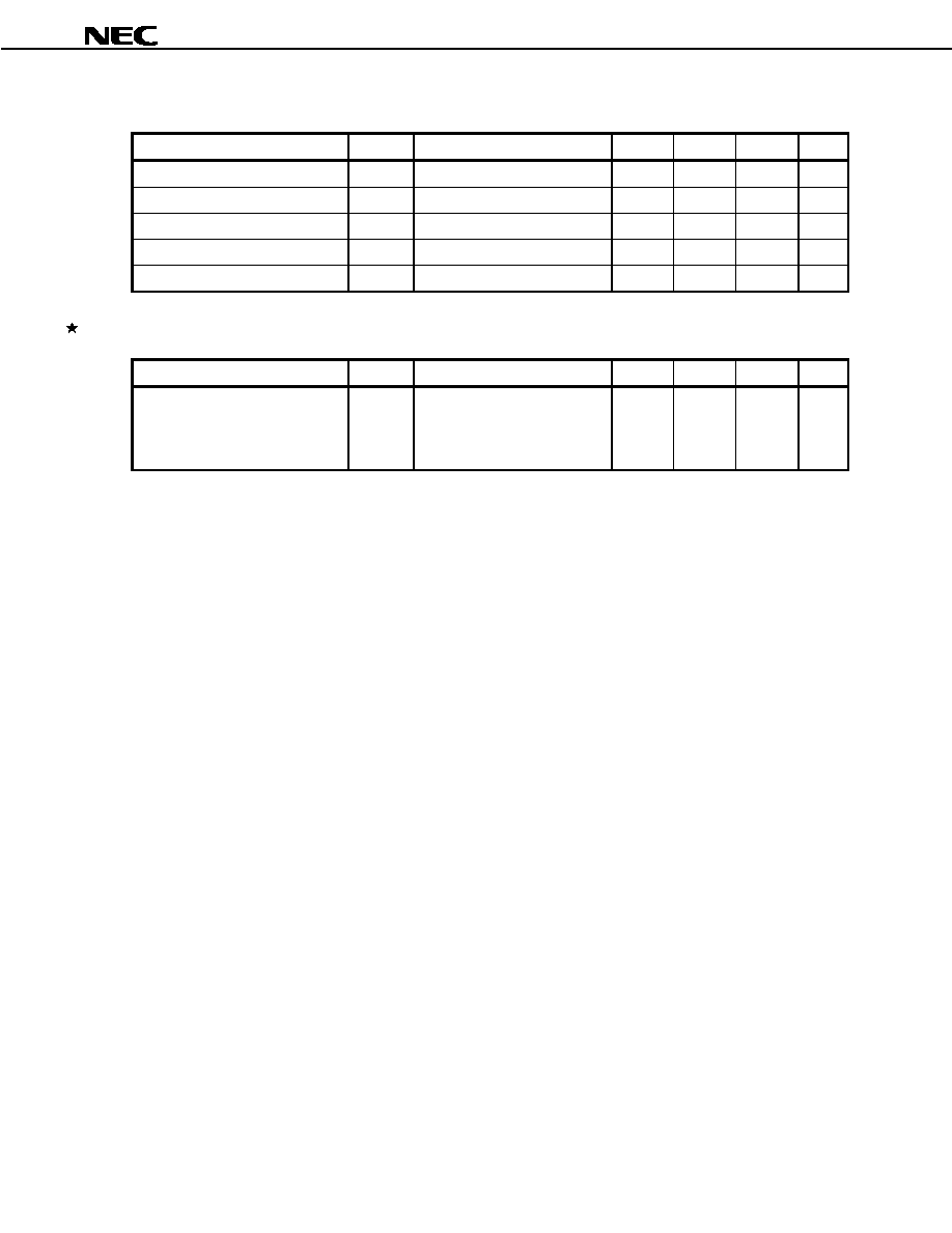
ORDERING INFORMATION
Part Number
Package
Á
PD98405GL-PMU
304-pin plastic QFP (0.5-mm fine pitch) (40
Î
40 mm)
Data Sheet S12689EJ2V0DS00
2
Á
Á
Á
Á
PD98405
SYSTEM CONFIGURATION EXAMPLE
PD98405
Á
EEPROM
TM
Expansion
ROM
PMD
Rx
Tx
ATM
network
Control
memory
PCI bus
ATM Interface Card
Data Sheet S12689EJ2V0DS00
3
Á
Á
Á
Á
PD98405
BLOCK DIAGRAM
PCI interface
Receive data FIFO (96 cells)
Receive controller
Sequencer
Transmit controller
Control memory interface
Control interface
Control memory
UTOPIA interface
DMA block
PMD
Host system
DMA output
block
Host command
FIFO
(10 commands)
DMA input
block
Transmit data
FIFO (10 cells)
Transmit
queue
buffer
(64 cells)
Receive
PHY
interface
Transmit
PHY
interface
Receive
ATM
interface
&
FIFO
(4 cells)
Receive
framer
Transmit
ATM
interface
&
FIFO
(4 cells)
Transmit
framer
PMD interface
& Clock recovery
& Clock synthesizer
Data Sheet S12689EJ2V0DS00
4
Á
Á
Á
Á
PD98405
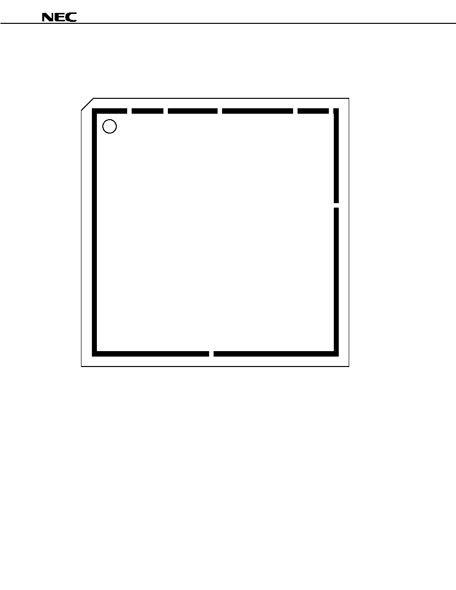
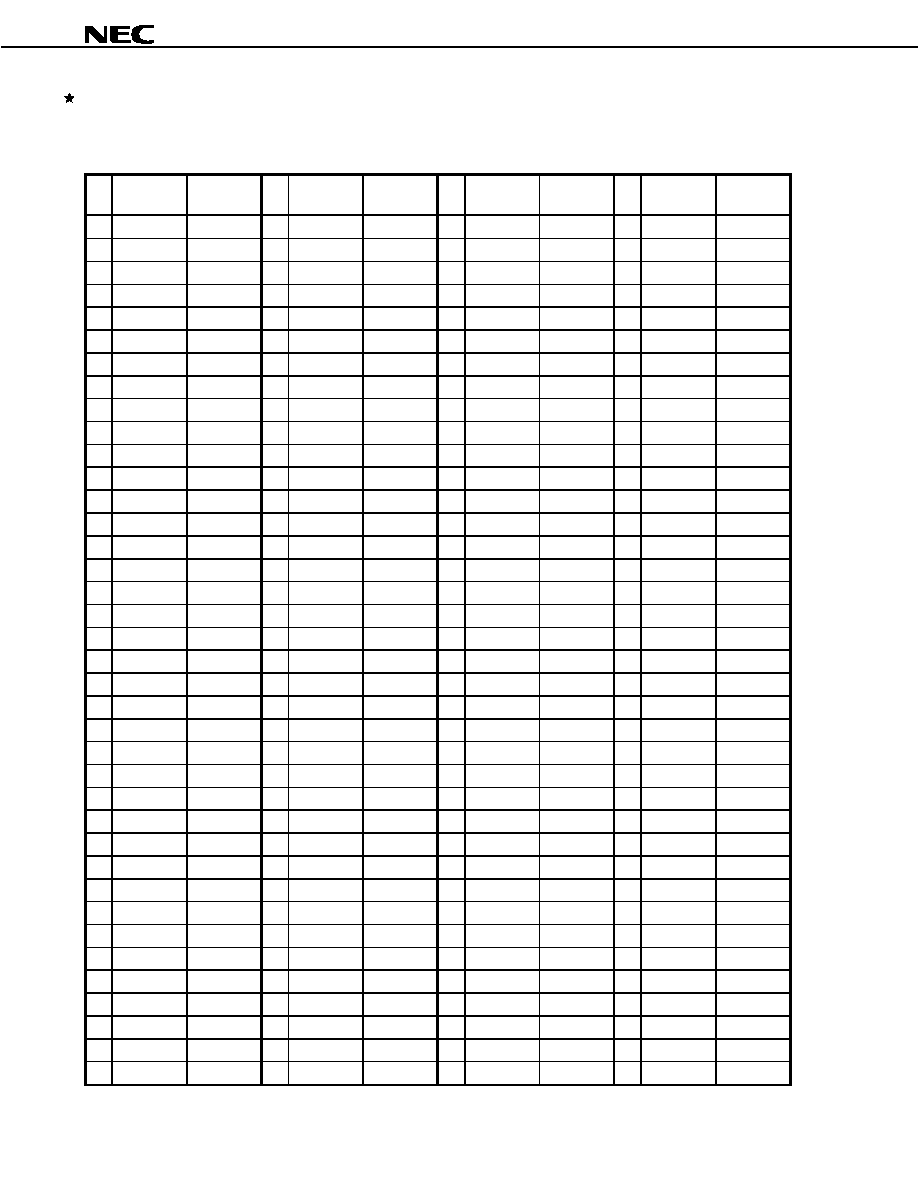
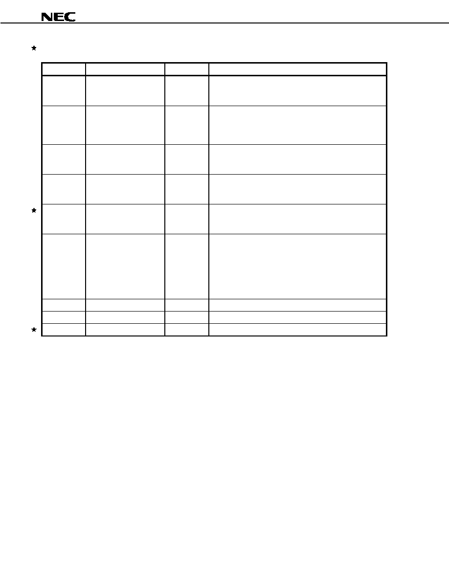
OUTLINE OF PINS
304-pin plastic QFP (0.5-mm fine pitch) (40
Î
Î
Î
Î
40 mm)
JTAG
PMD
PHY device
EEPROM
Expansion ROM
Control memory
PCI
PD98405GL-PMU
Á
304
229
1
228
153
76
77
152

Data Sheet S12689EJ2V0DS00
5
Á
Á
Á
Á
PD98405
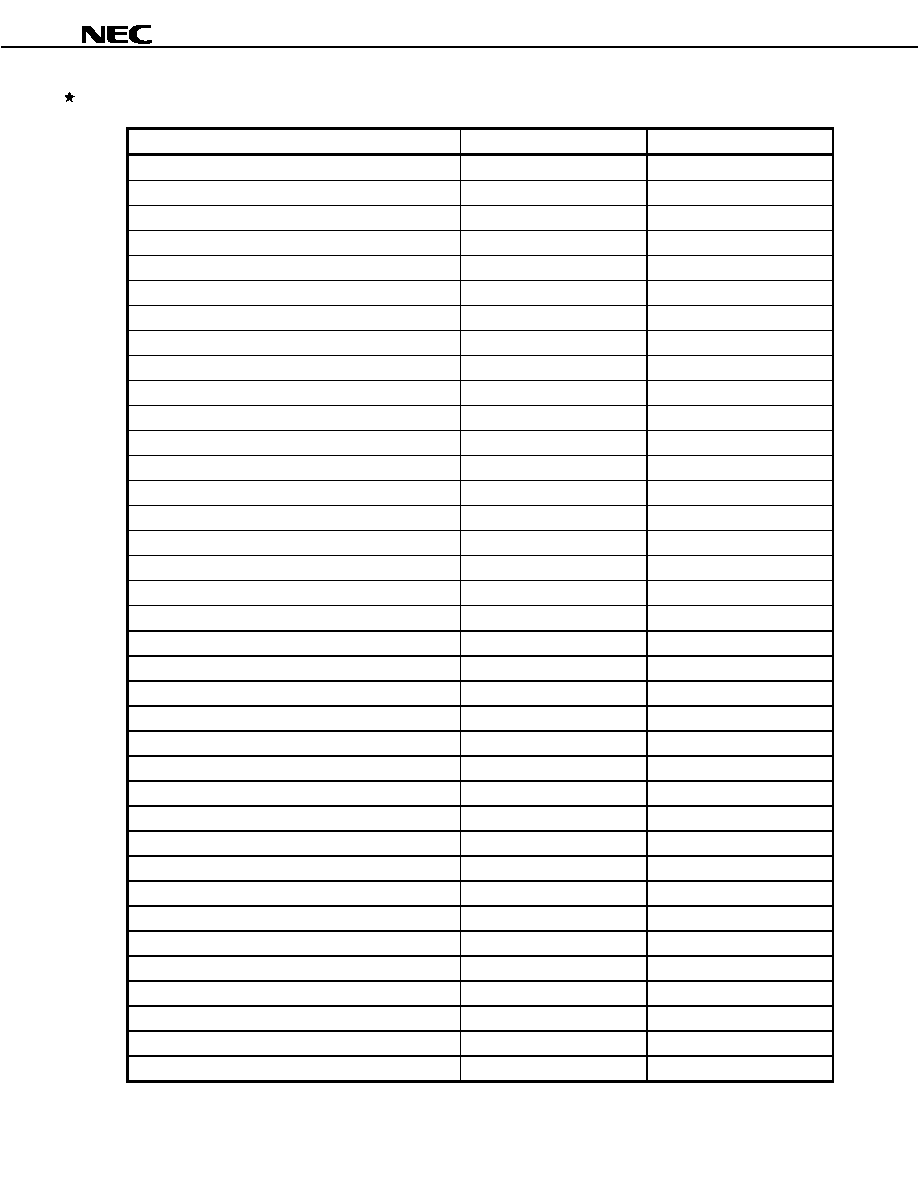
PIN NAME
ABRT_B
: Abort
PERR_B
: Parity Error
ACK64_B
: Acknowledge 64-bit Transfer
PHCE_B
: PHY Chip Enable
AD63-AD0
: Address/Data
PHINT_B
: PHY Interrupt
AGND
: Ground for Analog Part
PHOE_B
: PHY Output Enable
ASEL_B
: Slave Address Select
PHRST_B
: PHY Reset
ATTN_B
: Attention
PHR/W_B
: PHY Read/Write
AV
DD3
: +3.3 V Power Supply for
PHYALM
: Physical Alarm
Analog Part
RCLK
: Receive Clock
BE3_B-BE0_B
: Byte Enable
RCIC
: Receive Clock Input Complement
CA18-CA0
: Control Memory Address
RCIT
: Receive Clock Input True
CBE3_B-CBE0_B
: Local Port Byte Enable
RDIC
: Receive Data Input Complement
CD31-CD0
: Control Memory Data
RDIT
: Receive Data Input True
CLK
: Clock
PDY_B
: Target Ready
COE_B
: Control Memory Output Enable
REFCLK
: Reference Clock
CPAR3-CPAR0
: Control Memory parity
RENBL_B
: Receive Enable
CWE_B
: Control Memory Write Enable
REQ64_B
: Request 64-bit Transfer
DEVSEL_B
: Device Select
REQ_B
: Request
DR/W_B
: DMA Read/Write
RGND
: Ground for Receive PLL Part
EMPTY_B/RCLAV
: PHY Empty/Rx Cell Available
ROMA15-ROMA0 : Expansion ROM Address
ERR_B
: Error
ROMCS_B
: Expansion ROM Chip Select
E2PCLK
: Clock for EEPROM
ROMD7-ROMD0 : Expansion ROM Input Data
E2PCS
: EEPROM Chip Select
ROMOE_B
: Expansion ROM Output Enable
E2PDI
: Serial Data Input from EEPROM
RSOC
: Receive Start Cell
E2PDO
: Serial Data Output to EEPROM
RST_B
: Reset
FRAME_B
: Cycle Frame
RV
DD3
: +3.3 V Power Supply for Receive
FULL_B/TCLAV
: PHY Buffer full/Tx Cell Available
PLL Part
GND
: Ground for Digital Part
Rx7-Rx0
: Receive Data Bus
GNT_B
: Grant
SCLK
: SAR System Clock
HGND
: Ground for High-Speed Part
SD
: Signal Detect
HV
DD3
: +3.3 V Power Supply for
SEL_B
: Slave Select
High-Speed Part
SERR_B
: System Error
IDSEL
: ID Select
SIZE2-SIZE0
: Burst Size
INITD
: Initialization Disable
SR/W_B
: Slave Read /Write
INTR_B
: Interrupt
STOP_B
: Stop
IRDY_B
: Initiator Ready
TCLK
: Transmit Clock
JCK
: JTAG Test Pin
TDOC
: Transmit Data Output Complement
JDI
: JTAG Test Pin
TDOT
: Transmit Data Output True
JDO
: JTAG Test Pin
TENBL_B
: Transmit Enable
JMS
: JTAG Test Pin
TEST
: Test Mode Pin
JRST_B
: JTAG Test Pin
TFKC
: Transmit Reference Clock Complement
OE_B
: Output Enable
TFKT
: Transmit Reference Clock True
PAR
: Parity
TRDY_B
: Target Ready
PAR3-PAR0
: Bus Party
TSOC
: Transmit Start of Cell
PAR64
: Parity 64 bits
Tx7-Tx0
: Transmit Data Bus
PCBE7_B-PCBE0_B : Bus Command and Byte Enables
V
DD3
: +3.3 V Power Supply for Digital Part
PCI_MODE
: PCI Mode
V
DD5
: +5 V Power Supply for Digital Part
Data Sheet S12689EJ2V0DS00
6
Á
Á
Á
Á
PD98405
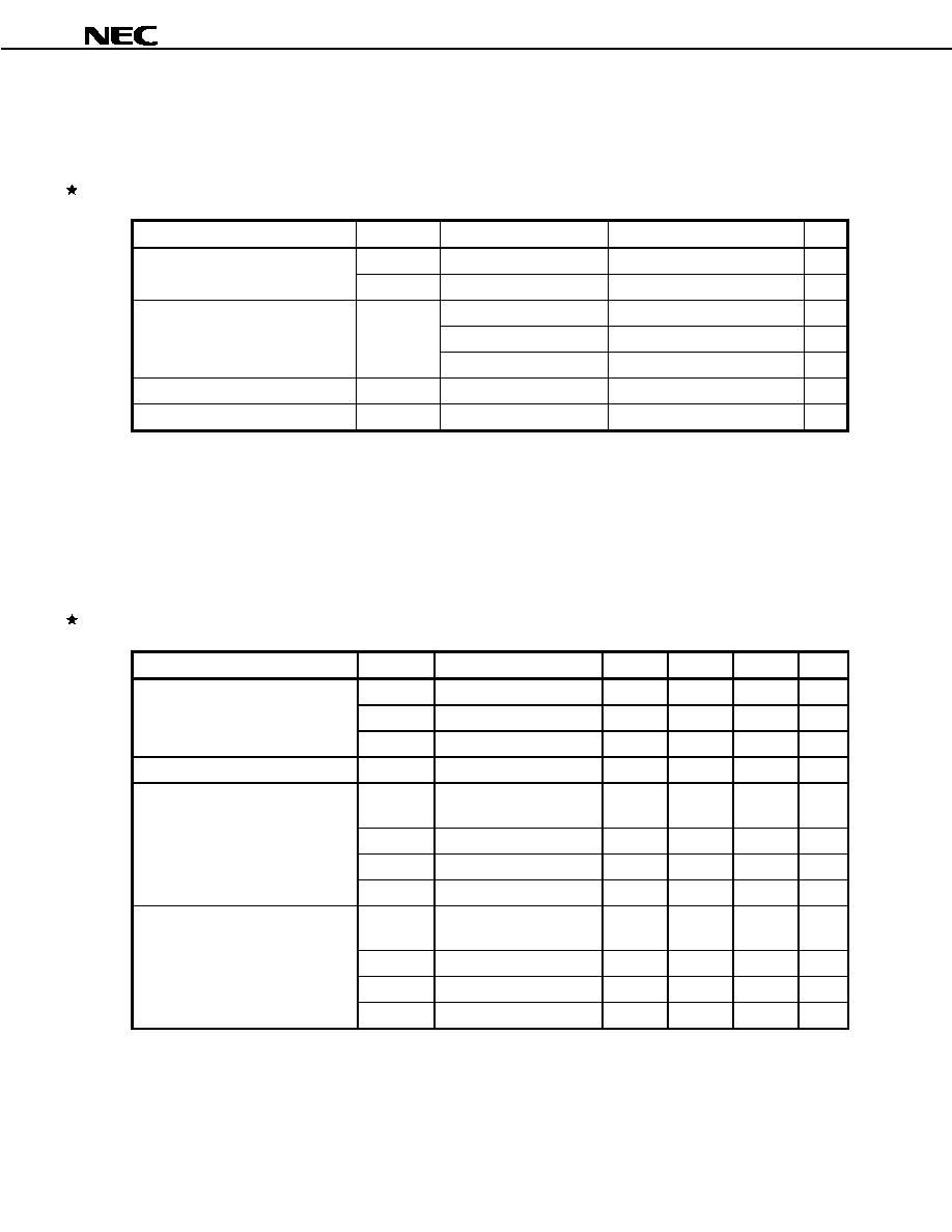
PIN CONFIGURATION
304-pin plastic QFP (0.5-mm fine pitch) (40
Î
Î
Î
Î
40 mm)
No.
PCI Mode
Generic
Mode
No.
PCI Mode
Generic
Mode
No.
PCI Mode
Generic
Mode
No.
PCI Mode
Generic
Mode
1
GND
GND
39
AD12
AD12
77
GND
GND
115 AD32
¡
2
V
DD3
V
DD3
40
AD11
AD11
78
V
DD3
V
DD3
116 PAR64
¡
3
AD24
AD24
41
AD10
AD10
79
AD57
¡
117 GND
GND
4
PCBE3_B
BE3_B
42
AD9
AD9
80
AD56
¡
118 PCI_MODE
PCI_MODE
5
IDSEL
¡
43
GND
GND
81
V
DD5
V
DD5
119 CD31
CD31
6
AD23
AD23
44
V
DD5
V
DD5
82
AD55
¡
120 CD30
CD30
7
GND
GND
45
AD8
AD8
83
AD54
¡
121 CD29
CD29
8
V
DD5
V
DD5
46
PCBE0_B
BE0_B
84
AD53
¡
122 CD28
CD28
9
AD22
AD22
47
AD7
AD7
85
AD52
¡
123 CD27
CD27
10
AD21
AD21
48
AD6
AD6
86
GND
GND
124 GND
GND
11
AD20
AD20
49
GND
GND
87
V
DD3
V
DD3
125 V
DD3
V
DD3
12
AD19
AD19
50
V
DD3
V
DD3
88
AD51
¡
126 CD26
CD26
13
GND
GND
51
AD5
AD5
89
AD50
¡
127 CD25
CD25
14
V
DD3
V
DD3
52
AD4
AD4
90
AD49
¡
128 CD24
CD24
15
AD18
AD18
53
AD3
AD3
91
AD48
¡
129 CD23
CD23
16
AD17
AD17
54
AD2
AD2
92
GND
GND
130 CD22
CD22
17
AD16
AD16
55
GND
GND
93
V
DD5
V
DD5
131 GND
GND
18
PCBE2_B
BE2_B
56
V
DD5
V
DD5
94
AD47
¡
132 CD21
CD21
19
GND
GND
57
AD1
AD1
95
AD46
¡
133 CD20
CD20
20
V
DD5
V
DD5
58
AD0
AD0
96
AD45
¡
134 CD19
CD19
21
FRAME_B
SEL_B
59
ACK64_B
OE_B
97
AD44
¡
135 CD18
CD18
22
IRDY_B
ASEL_B
60
REQ64_B
DR/W_B
98
GND
GND
136 CD17
CD17
23
TRDY_B
RDY_B
61
GND
GND
99
V
DD3
V
DD3
137 GND
GND
24
DEVSEL_B
SR/W_B
62
V
DD3
V
DD3
100 AD43
¡
138 V
DD3
V
DD3
25
GND
GND
63
PCBE7_B
SIZE2
101 AD42
¡
139 CD16
CD16
26
V
DD3
V
DD3
64
PCBE6_B
SIZE1
102 AD41
¡
140 CD15
CD15
27
STOP_B
ABRT_B
65
PCBE5_B
SIZE0
103 AD40
¡
141 CD14
CD14
28
PERR_B
ERR_B
66
PCBE4_B
PAR3
104 GND
GND
142 CD13
CD13
29
SERR_B
¡
67
V
DD5
V
DD5
105 V
DD5
V
DD5
143 CD12
CD12
30
PAR
¡
68
GND
GND
106 AD39
¡
144 CD11
CD11
31
GND
GND
69
AD63
PAR2
107 AD38
¡
145 GND
GND
32
V
DD5
V
DD5
70
AD62
PAR1
108 AD37
¡
146 CD10
CD10
33
PCBE1_B
BE1_B
71
AD61
PAR0
109 AD36
¡
147 CD9
CD9
34
AD15
AD15
72
V
DD3
V
DD3
110 GND
GND
148 CD8
CD8
35
AD14
AD14
73
AD60
¡
111 V
DD3
V
DD3
149 CD7
CD7
36
AD13
AD13
74
AD59
¡
112 AD35
¡
150 CD6
CD6
37
GND
GND
75
AD58
¡
113 AD34
¡
151 V
DD3
V
DD3
38
V
DD3
V
DD3
76
GND
GND
114 AD33
¡
152 GND
GND
Data Sheet S12689EJ2V0DS00
7
Á
Á
Á
Á
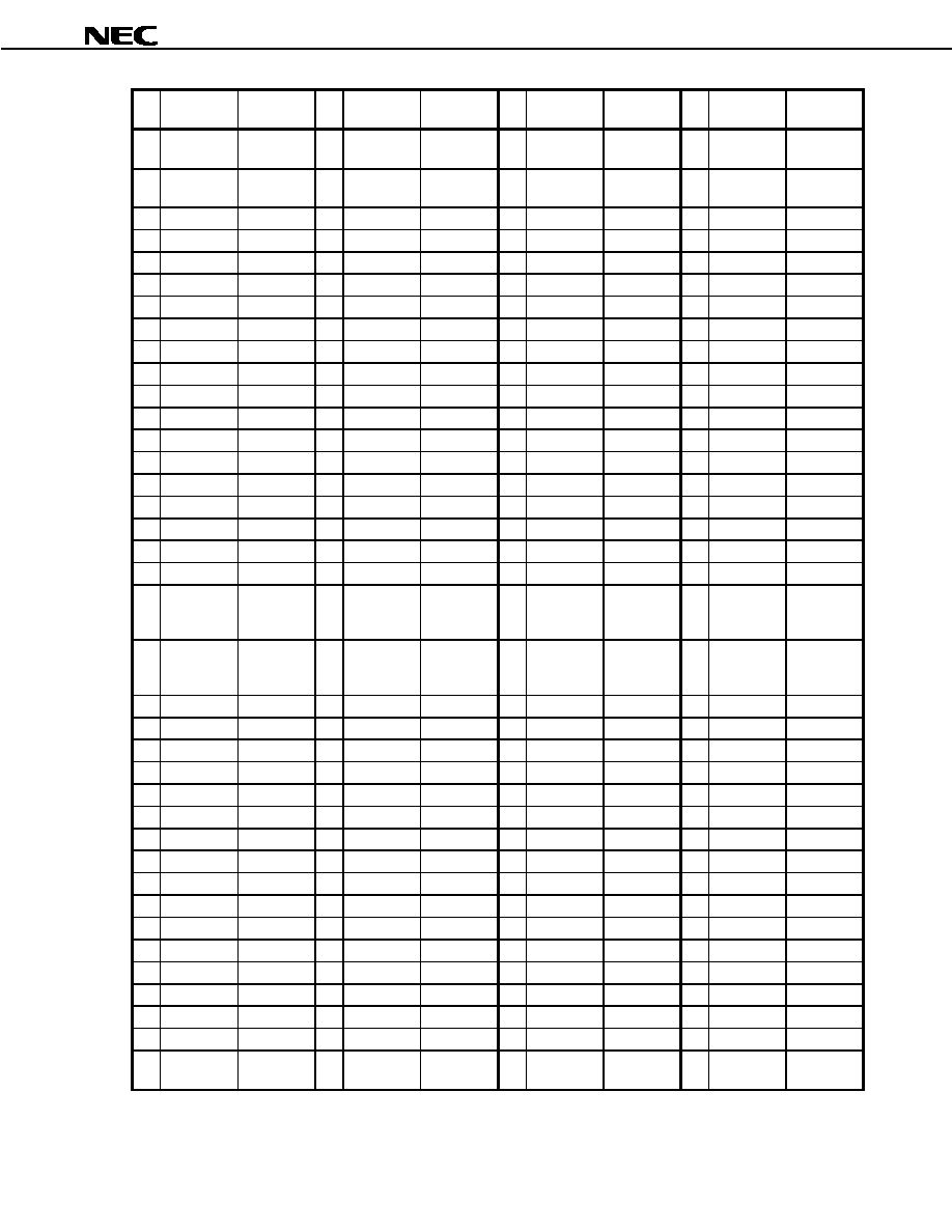
PD98405
No.
PCI Mode
Generic
Mode
No.
PCI Mode
Generic
Mode
No.
PCI Mode
Generic
Mode
No.
PCI Mode
Generic
Mode
153 GND
GND
191 CBE3_B
CBE3_B
229 GND
GND
267 SD/
PHCE_B
SD/
PHCE_B
154 V
DD3
V
DD3
192 CBE2_B
CBE2_B
230 ROMOE_B
¡
268 REFCLK/
PHINT_B
REFCLK/
PHINT_B
155 CD5
CD5
193 CBE1_B
CBE1_B
231 E2PDI
¡
269 AV
DD3
AV
DD3
156 CD4
CD4
194 CBE0_B
CBE0_B
232 E2PDO
¡
270 AGND
AGND
157 CD3
CD3
195 CWE_B
CWE_B
233 E2PCLK
¡
271 TEST
TEST
158 CD2
CD2
196 COE_B
COE_B
234 E2PCS
¡
272 HGND
HGND
159 CD1
CD1
197 INITD
INITD
235 Rx7
Rx7
273 TDOT
TDOT
160 GND
GND
198 SCLK
SCLK
236 Rx6
Rx6
274 TDOC
TDOC
161 CD0
CD0
199 GND
GND
237 Rx5
Rx5
275 HV
DD3
HV
DD3
162 CPAR3
CPAR3
200 ROMA15
¡
238 Rx4
Rx4
276 HV
DD3
HV
DD3
163 CPAR2
CPAR2
201 ROMA14
¡
239 Rx3
Rx3
277 RDIC
RDIC
164 CPAR1
CPAR1
202 ROMA13
¡
240 Rx2
Rx2
278 RDIT
RDIT
165 CPAR0
CPAR0
203 ROMA12
¡
241 Rx1/TFKC
Rx1/TFKC
279 HGND
HGND
166 CA18
CA18
204 ROMA11
¡
242 Rx0/TFKT
Rx0/TFKT
280 RV
DD3
RV
DD3
167 GND
GND
205 ROMA10
¡
243 GND
GND
281 JRST_B
JRST_B
168 CA17
CA17
206 ROMA9
¡
244 RCLK
RCLK
282 JCK
JCK
169 CA16
CA16
207 ROMA8
¡
245 V
DD3
V
DD3
283 JMS
JMS
170 CA15
CA15
208 V
DD3
V
DD3
246 RENBL_B
RENBL_B
284 JDO
JDO
171 CA14
CA14
209 ROMA7
¡
247 RSOC
RSOC
285 JDI
JDI
172 CA13
CA13
210 ROMA6
¡
248 EMPTY_B/
RCLAV/
RCIC
EMPTY_B/
RCLAV/
RCIC
286 RGND
RGND
173 CA12
CA12
211 ROMA5
¡
249 FULL_B/
TCLAV/
RCIT
FULL_B/
TCLAV/
RCIT
287 V
DD5
V
DD5
174 GND
GND
212 ROMA4
¡
250 TSOC
TSOC
288 INTR_B
INTR_B
175 V
DD3
V
DD3
213 ROMA3
¡
251 TENBL_B
TENBL_B
289 RST_B
RST_B
176 CA11
CA11
214 GND
GND
252 GND
GND
290 CLK
CLK
177 CA10
CA10
215 ROMA2
¡
253 TCLK
TCLK
291 GNT_B
GNT_B
178 CA9
CA9
216 ROMA1
¡
254 V
DD3
V
DD3
292 GND
GND
179 CA8
CA8
217 ROMA0
¡
255 Tx7
Tx7
293 V
DD3
V
DD3
180 CA7
CA7
218 ROMD7
¡
256 Tx6
Tx6
294 REQ_B
REQ_B
181 CA6
CA6
219 ROMD6
¡
257 Tx5
Tx5
295 AD31
AD31
182 GND
GND
220 ROMD5
¡
258 Tx4
Tx4
296 AD30
AD30
183 CA5
CA5
221 ROMD4
¡
259 GND
GND
297 AD29
AD29
184 CA4
CA4
222 ROMD3
¡
260 Tx3
Tx3
298 GND
GND
185 CA3
CA3
223 ROMD2
¡
261 Tx2
Tx2
299 V
DD5
V
DD5
186 CA2
CA2
224 ROMD1
¡
262 Tx1
Tx1
300 AD28
AD28
187 CA1
CA1
225 ROMD0
¡
263 Tx0
Tx0
301 AD27
AD27
188 CA0
CA0
226 ROMCS_B
¡
264 PHRST_B
PHRST_B
302 AD26
AD26
189 GND
GND
227 V
DD3
V
DD3
265 PHOE_B
PHOE_B
303 AD25
AD25
190 V
DD3
V
DD3
228 GND
GND
266 PHYALM/
PHR/W_B
PHYALM/
PHR/W_B
304 GND
GND
Remark Open the pins to which no function is allocated (pins marked "¡" in the Generic Mode column in the
above table) in the Generic mode. Fix pin 5 (IDSEL) to the low/high level.

Data Sheet S12689EJ2V0DS00
8
Á
Á
Á
Á
PD98405
CONTENTS
1. PIN FUNCTIONS ...............................................................................................................................
9
1.1 PHY Layer Device Interface Signal ..........................................................................................
9
1.1.1
UTOPIA interface ...........................................................................................................................
9
1.1.2
PHY device control interface (external PHY mode, PHM of GMR register = 1) .............................
11
1.2 Bus Interface Signals ................................................................................................................
12
1.2.1
Generic bus interface signals (PCI_MODE pin: low level).............................................................
12
1.2.2
PCI bus interface signal (PCI_MODE pin: high level)....................................................................
15
1.3 Control Memory Interface Signals ...........................................................................................
19
1.4 PMD Interface Signals (internal PHY mode, PHM of GMR register = 0) ...............................
20
1.5 JTAG Boundary Scan Signals ..................................................................................................
21
1.6 Other Signals .............................................................................................................................
21
1.7 Power and Ground.....................................................................................................................
22
1.8 Pin Status during and after Reset ............................................................................................
23
2. ELECTRICAL SPECIFICATIONS .....................................................................................................
25
3. PACKAGE DRAWING ......................................................................................................................
60
4. RECOMMENDED SOLDERING CONDITIONS ...............................................................................
61
Data Sheet S12689EJ2V0DS00
9
Á
Á
Á
Á
PD98405
1. PIN FUNCTIONS
The package of the
Á
PD98405 has 304 pins. For details on how to use each pin, refer to
Á
Á
Á
Á
PD98405 User's
Manual (S12250E).
1.1 PHY Layer Device Interface Signal
The PHY Layer device interfaces include a UTOPIA interface by which the
Á
PD98405 exchanges ATM cells with a
PHY device, and PHY control interface that is used to control a PHY device. The
Á
PD98405 supports two types of
PHY layer device interfaces: UTOPIA octet and cell level. These modes are selected by setting the UOC bit of the
GMR register.
The PHY layer device interface signals are for an external PHY layer device. When using an internal PHY layer,
open all the pins except the common pins. Even when the internal PHY layer is used, an external receive FIFO can
be connected to the
Á
PD98405 via the UTOPIA interface.
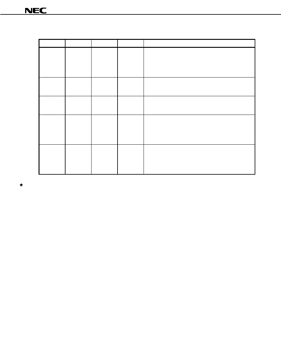
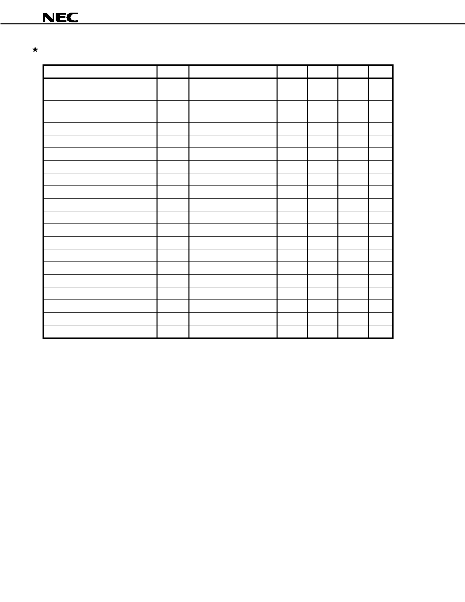
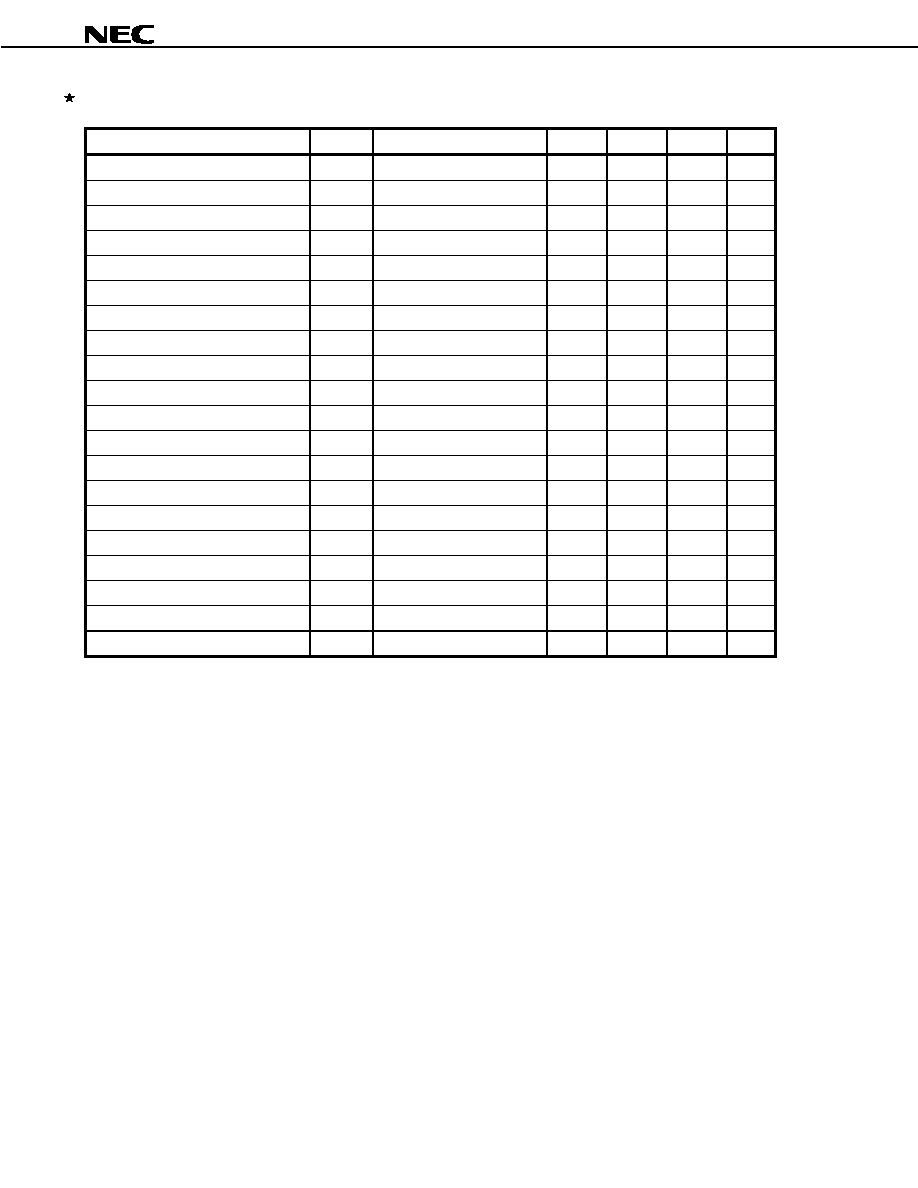
1.1.1 UTOPIA interface
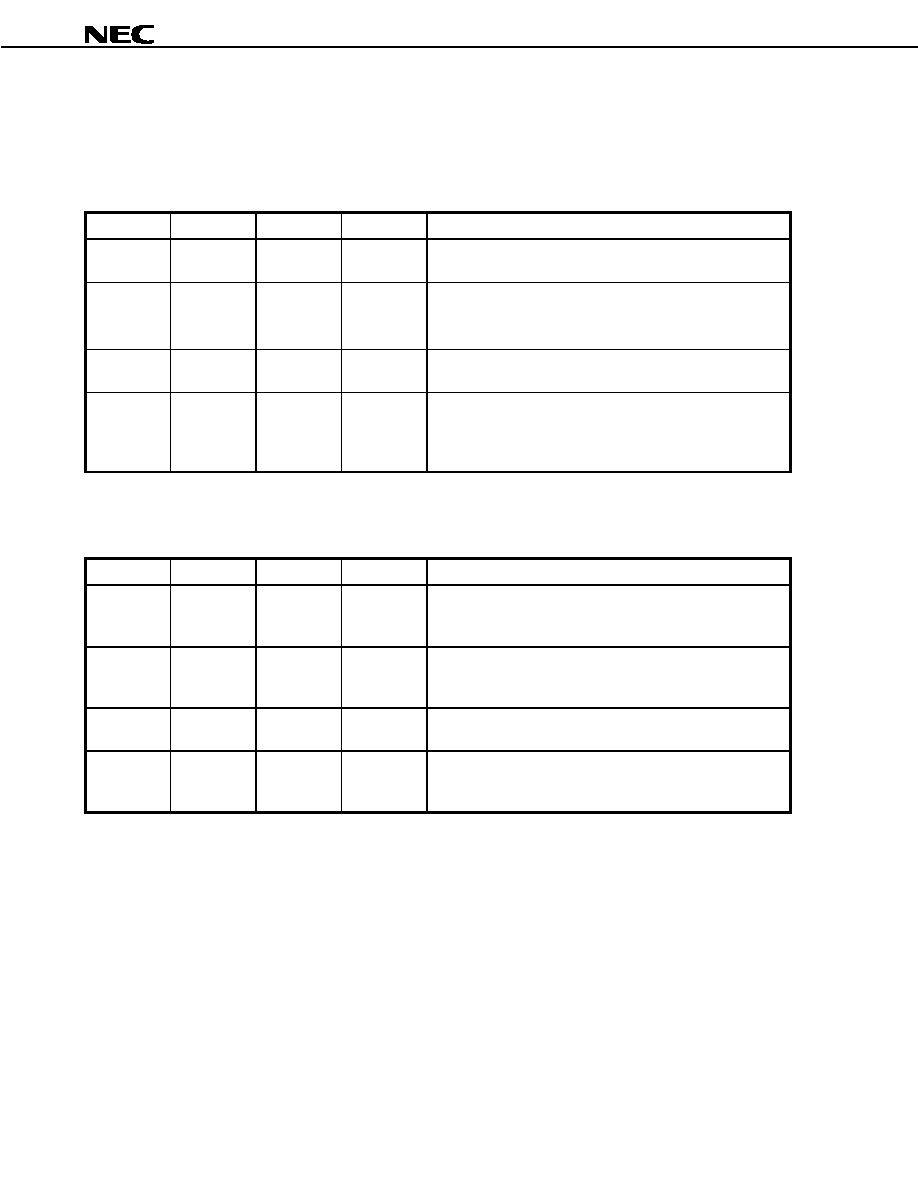
(1/2)
Pin Name
Pin No.
I/O
I/O Level
Function
Rx7-Rx0
(Rx1 and
Rx0: Shared
with TFKC
and TFKT)
235-242
I
TTL
Receive data bus.
These pins constitute an 8-bit input bus that inputs receive data
from the network to the
Á
PD98405 from the PHY layer device in
byte format. The
Á
PD98405 reads the data on this bus in
synchronization with the rising edge of RCLK. Rx7 through Rx2
are internally pulled down.
Open the pins of this bus when they are not used. Pull up Rx1
when it is not used, and pull down Rx0 when it is not used.
RSOC
247
I
TTL
Receive cell start position.
This signal is input from the PHY layer device in synchronization
with the first byte of cell data. It is high while the first byte of a
header is input to Rx7 through Rx0.
This signal is internally pulled down.
RENBL_B
246
O
TTL
Receive enable.
This signal informs the PHY layer device that the
Á
PD98405 is
ready to receive data in the next clock cycle.
Data Sheet S12689EJ2V0DS00
10
Á
Á
Á
Á
PD98405
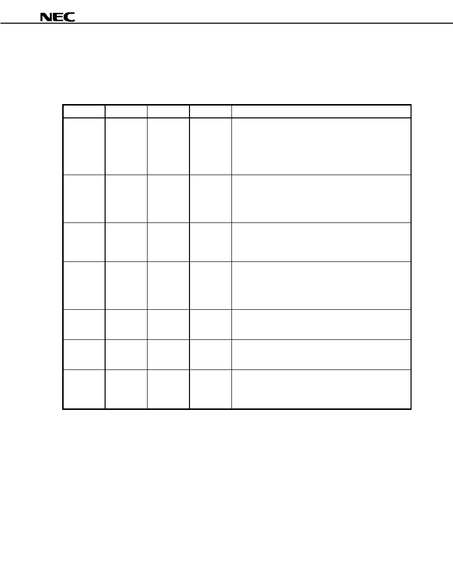
(2/2)
Pin Name
Pin No.
I/O
I/O Level
Function
EMPTY_B/
RCLAV
(shared with
RCIC)
248
I
TTL
PHY layer buffer empty/receive cell available.
This signal informs the
Á
PD98405 that the PHY receive FIFO
has no cell data to be transferred and that the PHY device
cannot supply receive data. This signal functions as EMPTY_B
when the UTOPIA interface is in the octet level handshake
mode, to indicate that the data on Rx7 through Rx0 is invalid in
the current clock cycle. In the cell level handshake mode, it
functions as RCLAV, informing the
Á
PD98405 that no more
cells are to be supplied after transfer of the current cell is
completed.
Pull down this pin when it is not used.
RCLK
244
O
TTL
Receive clock.
This clock is used for synchronization when the
Á
PD98405
transfers cell data to and from the PHY layer device at the
reception side. The SAR system clock input to the SCLK pin is
output from this pin as is, immediately after the
Á
PD98405 has
been reset.
Tx7-Tx0
255-258,
260-263
O
TTL
Transmit data bus.
These pins form an 8-bit output bus that outputs data to be
transmitted to the network, to the PHY layer device in byte
format. The
Á
PD98405 outputs the data in synchronization with
the rising edge of TCLK.
TSOC
250
O
TTL
Transmit cell start position.
This signal is output in synchronization with the first byte of
transmit cell data.
TENBL_B
251
O
TTL
Transmit enable.
This signal informs the PHY layer device that data has been
output to Tx7 through Tx0 in the current clock cycle.
FULL_B/
TCLAV
(shared with
RCIT)
249
I
TTL
PHY layer buffer full/transmit cell available.
The FULL_B signal informs the
Á
PD98405 that the input buffer
of the PHY device is full and that the device can receive no
more data. When the UTOPIA interface is in the octet level
handshake mode, the PHY device inputs an inactive level as
this signal if the device can receive cell data. In the cell level
handshake mode, this signal functions as TCLAV, informing the
Á
PD98405 that the PHY device can receive the next single cell
after transfer of the current cell is completed.
Pull up this pin when it is not used.
TCLK
253
O
TTL
Transmit clock.
This clock is used for synchronization when the
Á
PD98405
transfers cell data to and from the PHY layer device at the
transmission side. The SAR system clock input to the SCLK pin
is output as this clock as is.
Data Sheet S12689EJ2V0DS00
11
Á
Á
Á
Á
PD98405
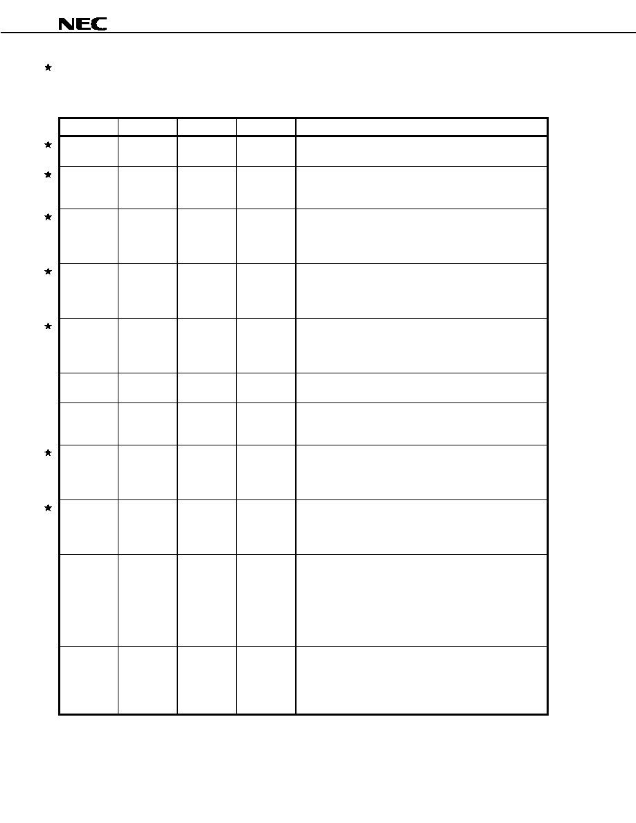
1.1.2 PHY device control interface (external PHY mode, PHM of GMR register = 1)
Pin Name
Pin No.
I/O
I/O Level
Function
PHR/W_B
(shared with
PHYALM)
266
O
TTL
PHY read/write.
The
Á
PD98405 indicates the PHY layer device control direction
by using this pin.
1: Read
0: Write
PHOE_B
265
O
TTL
PHY layer output enable.
The
Á
PD98405 enables output by the PHY layer device by
making this signal low.
PHCE_B
(shared with
SD)
267
O
TTL
PHY layer chip enable.
The
Á
PD98405 makes this signal low when it accesses the PHY
layer device.
PHINT_B
(shared with
REFCLK)
268
I
TTL
PHY layer interrupt.
This pin inputs an interrupt signal to the
Á
PD98405 from the
PHY layer device. The PHY layer device informs the
Á
PD98405
that it has an interrupt source by inputting a low level to this pin.
Pull up this pin when it is not used.
PHRST_B
264
O
TTL
PHY layer reset.
This signal is used to reset the PHY layer device. The
Á
PD98405 keeps this pin low for the duration of 17 clock cycles
when a low level is input to the RST_B pin or when software
reset is executed.
Caution The PHCE_B/SD pins are multiplexed pins and their functions differ depending on whether the
internal PHY mode or external PHY mode is selected (by using the PHM bit of the GMR register).
Because the PHCE_B/SD pins change the mode between input and output depending on the
selected mode, be sure to correctly set the PHM bit of the GMR register.
Data Sheet S12689EJ2V0DS00
12
Á
Á
Á
Á
PD98405
1.2 Bus Interface Signals
The
Á
PD98405 supports a PCI bus interface or generic bus interface. Whether the PCI bus interface or generic
bus interface is to be supported is selected by the PCI_MODE signal.
The PCI bus interface can be directly connected to a PCI bus. The generic bus interface can be connected to a
general I/O bus with a few circuits.
1.2.1 Generic bus interface signals (PCI_MODE pin: low level)
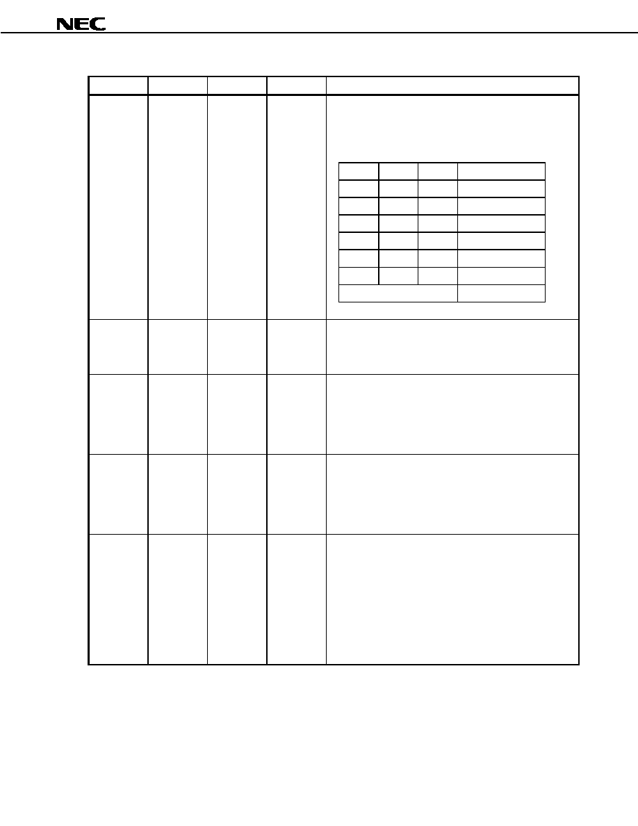
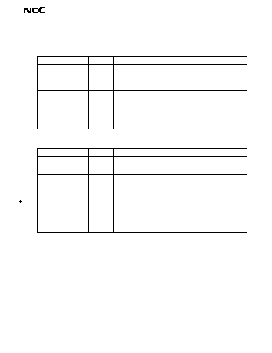
(1/3)
Pin Name
Pin No.
I/O
I/O Level
Function
AD31-AD0
295-297,
300-303,
3, 6, 9-12,
15-17,
34-36,
39-42,
45, 47, 48,
51-54,
57-58
I/O
3-state
TTL
Address/data.
These pins constitute a 32-bit address/data bus. They are
input/output pins multiplexing an address bus and a data bus.
An address is transferred at the first input/output clock. From
the second clock and onward, data is transferred. When the
Á
PD98405 is not accessing the bus, the AD bus goes into a
high-impedance state.
BE3_B
BE2_B
BE1_B
BE0_B
4
18
33
46
O
3-state
TTL
Byte enable.
These pins determine the byte that becomes valid in the master
cycle of the
Á
PD98405. BE3_B corresponds to AD31 through
AD24, and BE0_B corresponds to AD7 through AD0. BE3_B
through BE0_B go into a high-impedance state when the
Á
PD98405 is not accessing a bus or when it is accessing a
slave.
PAR3
PAR2
PAR1
PAR0
66
69
70
71
I/O
3-state
TTL
Bus parity.
These pins indicate the parity of AD31 through AD0. A parity
check mode is set by the GMR register. Whether the parity is
enabled or disabled, whether an odd parity or even parity is
used, and whether a word parity or byte parity is used can be
specified. When byte parity is used, PAR3 indicates the parity
of AD31 through AD24, and PAR0 indicates the parity of AD7
through AD0. In the case of word parity, PAR2 through PAR0
do not function, and PAR3 serves as an input/output pin. These
pins function as output pins when an address is output and
when data is written, and as input pins when data is read.
When the
Á
PD98405 is not accessing a bus, PAR3 through
PAR0 go into a high-impedance state. Pull up these pins when
they are not used.
OE_B
59
I
TTL
Output enable.
When this pin is low, the
Á
PD98405 allows AD31 through AD0
and PAR3 through PAR0 to operate normally as three-state I/O
pins. These pins go into a high-impedance state while a high
level is input to this pin. Fix this pin to the low level in a system
where the above pins do not have to forcibly go into a high-
impedance state.
Data Sheet S12689EJ2V0DS00
13
Á
Á
Á
Á
PD98405
(2/3)
Pin Name
Pin No.
I/O
I/O Level
Function
SIZE2
SIZE1
SIZE0
63
64
65
O
TTL
Burst size.
These pins indicate the size of current DMA transfer. They are
used to interface with a bus (such as S bus) that requires an
explicit burst size.
SIZE2
SIZE1
SIZE0
Function
0
0
0
1-word transfer
0
0
1
2-word burst
0
1
0
4-word burst
0
1
1
8-word burst
1
0
0
16-word burst
1
0
1
12-word burst
Others
Undefined
DR/W_B
60
O
TTL
DMA read/write.
This pin indicates the direction of DMA access.
1: Read access
0: Write access
ATTN_B
294
O
TTL
Attention (DMA request).
The
Á
PD98405 makes the ATTN_B signal low when it is to
execute a DMA operation. The ATTN_B signal becomes
inactive in synchronization with the rising edge of CLK when
only one more word of data is to be transferred by means of
DMA.
GNT_B
291
I
TTL
Bus enable.
The GNT_B signal goes low when the bus arbiter grants the
Á
PD98405 the bus mastership in response to a DMA request
from the
Á
PD98405. When the
Á
PD98405 detects that the
GNT_B signal has gone low, it starts a DMA operation,
assuming that the bus mastership has been granted.
RDY_B
23
I
TTL
Target device ready.
This signal informs the
Á
PD98405 in the DMA cycle that the
target device is ready for input/output. The
Á
PD98405 makes
the RDY_B signal low if valid data exists on AD31 through AD0
when it executes a DMA read operation. When executing a
DMA write operation, the
Á
PD98405 makes the ATTN_B signal
low if the target device is ready for reception.
The timing at which the
Á
PD98405 samples the RDY_B and
ABRT_B signals can be bring forward by 1 clock depending on
the setting of an internal register (GMR register).

Data Sheet S12689EJ2V0DS00
14
Á
Á
Á
Á
PD98405
(3/3)
Pin Name
Pin No.
I/O
I/O Level
Function
ABRT_B
27
I
TTL
Abort.
This signal is used to abort a data transfer cycle. If this signal
goes low in the middle of a data transfer cycle, that cycle is
aborted, and the
Á
PD98405 resumes burst starting from the
aborted data. While a low level is input to ABRT_B, the RDY_B
signal does not function. The user can bring forward the timing
at which the
Á
PD98405 samples the RDY_B and ABRT_B
signals by 1 clock (early mode) by using an internal register
(GMR register). Pull up this pin when it is not used.
ERR_B
28
I
TTL
System bus error.
If an error is detected on the system bus, the device that
manages the bus uses this pin to stop the operation by the
Á
PD98405.
When a low level is input to this pin, the
Á
PD98405 stops all bus
operations, sets the system bus error bit (bit 25) of the GSR
register (when not masked), and generates an interrupt. Pull up
this pin when it is not used.
SR/W_B
24
I
TTL
Slave read/write.
This signal determines the direction of slave access.
1: Read access
0: Write access
SEL_B
21
I
TTL
Slave select.
This signal is asserted active (low) when slave access is
selected for the
Á
PD98405. Make sure that the SEL_B signal
goes low at the same time as or after the ASEL_B signal has
gone low. In addition, insert an inactive period of two system
clocks or more after the SEL_B signal has become inactive and
before it becomes active next time.
ASEL_B
22
I
TTL
Slave address select.
The ASEL_B signal selects the direct address register of the
Á
PD98405.
When a low level is input to ASEL_B, the
Á
PD98405 samples
the AD bus at the first rising edge of CLK.
CLK
290
I
TTL
Clock.
This is a system bus clock input pin. A clock of up to 33 MHz
can be input.
RST_B
289
I
TTL
Reset.
The RST_B signal initializes the
Á
PD98405 (on starting). After
reset, the
Á
PD98405 can start normal operation. When a low
level is input to RST_B, the internal state machine and registers
of the
Á
PD98405 are reset, and all the three-state signals go
into a high-impedance state. Reset input is asynchronous. If it
is input during operation, the operation status at that time is lost.
Keep RST_B low at least for the duration of one clock cycle.
INTR_B
288
O
N-ch
open-drain
Interrupt output.
Pull up this signal because it is an open-drain signal.
This signal informs the CPU that an unmasked interrupt bit of
the interrupt GSR register has been set.

Data Sheet S12689EJ2V0DS00
15
Á
Á
Á
Á
PD98405
1.2.2 PCI bus interface signal (PCI_MODE pin: high level)
The
Á
PD98405 has a 32-/64-bit PCI bus interface. This bus interface can be directly connected to a PCI bus. In
addition, the
Á
PD98405 also has a serial EEPROM interface and an expansion ROM interface.
<1>
PCI bus interface signals
(1/2)
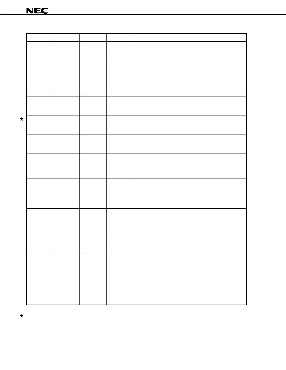
Pin Name
Pin No.
I/O
I/O Level
Function
AD31-AD0
295-297,
300-303,
3, 6, 9-12,
15-17,
34-36,
39-42,
45, 47, 48,
51-54,
57-58
I/O
3-state
PCI
Address/data.
AD31 through AD0 constitute a 32-bit multiplexed address/data
bus. When the
Á
PD98405 operates as a bus master, it drives
an address at the first clock and transfers data at the second
clock and onward.
PCBE3_B
PCBE2_B
PCBE1_B
PCBE0_B
4
18
33
46
I/O
3-state
PCI
Bus command/byte enable.
These signals define a "bus command" (bus transaction that
occurs) in the address phase. In the data phase, they indicate
which byte lane holds valid data. The PCBE3_B pin
corresponds to byte 3 (bits 31 through 24), and PCBE0_B pin
corresponds to byte 0 (bits 7 through 0).
PAR
30
I/O
3-state
PCI
Parity.
This signal indicates an even parity on the AD31 through AD0
and PCBE3_B through PCBE0_B pins, including the PAR
signal. When the
Á
PD98405 is operating as a master, the PAR
signal becomes active in the address and write data phases.
When the
Á
PD98405 is operating as a target, this signal
becomes active in the read data phase.
FRAME_B
21
I/O
Sustained
3-state
PCI
Frame.
This signal indicates the start and period of a bus transaction.
When this signal is asserted active, it indicates the start of a bus
transaction. While it is active, data is transferred. It is
deasserted inactive when the next data transfer phase will
transfer last data of the transaction.
TRDY_B
23
I/O
Sustained
3-state
PCI
Target ready.
This signal goes low when the target device is ready to
complete the transaction of the current data. This signal is used
in combination with IRDY_B, and read/write data transfer is
executed when both IRDY_B and TRDY_B signals are low.
IRDY_B
22
I/O
Sustained
3-state
PCI
Initiator ready.
This signal goes low when the initiator is ready to complete the
transaction of the current data. This signal is used in
combination with TRDY_B, and read/write data transfer is
executed when both IRDY_B and TRDY_B are low.
If FRAME_B and IRDY_B are both inactive, the bus cycle is not
executed. A wait cycle is inserted until both IRDY_B and
TRDY_B are asserted active.
Data Sheet S12689EJ2V0DS00
16
Á
Á
Á
Á
PD98405
(2/2)
Pin Name
Pin No.
I/O
I/O Level
Function
STOP_B
27
I/O
Sustained
3-state
PCI
Stop.
This signal goes low when the target device requests the master
device to stop the current transaction.
DEVSEL_B
24
I/O
Sustained
3-state
PCI
Device select.
When the
Á
PD98405 is operating as a target, it makes this
signal low after the FRAME_B signal has been asserted active
and the
Á
PD98405 has recognized an address. When the
Á
PD98405 is operating as a master, it samples this signal to
check to see if a target device has been selected.
IDSEL
5
I
PCI
Initialization device select.
This signal is high when the configuration register of the
Á
PD98405 is read or written.
REQ_B
294
O
Note
PCI
Request.
The
Á
PD98405 makes this signal low to request the arbiter for
the bus mastership.
GNT_B
291
I
PCI
Grant.
This signal goes low when the arbiter grants the
Á
PD98405 the
bus mastership.
PERR_B
28
I/O
Sustained
3-state
PCI
Parity error.
This signal indicates that the
Á
PD98405 has detected a data
parity error. It is enabled when the "Parity Error Response" bit of
the configuration register is set to "1".
SERR_B
29
O
N-ch
open-drain
System error.
This signal indicates that the
Á
PD98405 has detected an
address parity error. It is enabled when both the "Parity Error
Response" and "System Error Enable" bits of the configuration
register are set to "1".
INTR_B
288
O
N-ch
open-drain
Interrupt output.
Pull up this signal because it is an open-drain signal. INTR_B
informs the CPU that an unmasked interrupt bit of the interrupt
GSR register has been set.
CLK
290
I
PCI
Clock.
This is a system bus clock input pin. A clock of up to 33 MHz is
input.
RST_B
289
I
PCI
Reset.
This signal initializes the
Á
PD98405 (on starting, etc.).
When a low level is input to RST_B, the internal state machine
and registers of the
Á
PD98405 are reset, and all the three-state
signals go into a high-impedance state. The reset input is
asynchronous. When this signal is input during operation, the
operating status at that time is lost. Keep RST_B low at least
for the duration of one clock cycle. After reset, do not access
the
Á
PD98405 for the duration of at least 20 clocks.
Note According to "PCI Local Bus Specification Revision 2.1", the REQ_B pin should go into a high-impedance
state while a low level is input to the RST_B pin. The REQ_B pin of the
Á
PD98405, however, outputs a
high level.

Data Sheet S12689EJ2V0DS00
17
Á
Á
Á
Á
PD98405
<2>
PCI bus 64-bit expansion interface signals
Open AD63 through AD32, PCBE7_B through PCBE4_B, and PAR64 when using the 32-bit PCI bus interface.
Pin Name
Pin No.
I/O
I/O Level
Function
AD63-AD32
69-71,
73-75, 79, 80,
82-85,
88-91,
94-97,
100-103,
106-109,
112-115
I/O
3-state
PCI
Address/data.
AD63 through AD32 constitutes a 32-bit multiplexed
address/data bus that extends the PCI bus to 64 bits. This
address/data bus transfers the high-order 32 bits of a 64-bit
address in the address phase. It outputs the high-order 32 bits
of 64-bit data in the data phase when both REQ64_B and
ACK64_B are asserted.
PCBE7_B
PCBE6_B
PCBE5_B
PCBE4_B
63
64
65
66
I/O
3-state
PCI
Bus command/byte enable.
These signals define a "bus command" (bus transaction that
occurs) in the address phase. In the data phase, they indicate
which byte lane holds valid data. The PCBE7_B pin
corresponds to AD63 through AD56, and PCBE4_B pin
corresponds to AD39 through AD32.
PAR64
116
I/O
3-state
PCI
Parity 64.
This signal indicates an even parity on AD63 through AD32 and
PCBE7_B through PCBE4_B pins, including the PAR64 signal.
When the
Á
PD98405 is operating as a master, the PAR signal
becomes active in the address and write data phases. When
the
Á
PD98405 is operating as a target, it becomes active in the
read data phase.
REQ64_B
60
I/O
3-state
PCI
Request 64.
This signal indicates the start and period of a 64-bit bus
transaction. When the
Á
PD98405 is operating as a master, it
asserts REQ64_B active to request 64-bit data transfer.
REQ64_B is the same as FRAME_B in timing.
ACK64_B
59
I/O
Sustained
3-state
CPI
Acknowledge 64.
When the
Á
PD98405 is operating as a target, it makes this
signal low after the REQ64_B signal has been asserted active
and the
Á
PD98405 has recognized an address. When the
Á
PD98405 is operating as a master, it samples this signal to
check whether the target device has acknowledged 64-bit
transfer. ACK64_B is the same as DEVSEL_B in timing.
Data Sheet S12689EJ2V0DS00
18
Á
Á
Á
Á
PD98405
<3>
Serial EEPROM interface signals
The
Á
PD98405 has a serial EEPROM interface supporting MICROWIRE
TM
interface. Through this serial
EEPROM interface, the contents of the PCI configuration register can be loaded from an EEPROM connected.
Remark It is recommended that National Semiconductor's "NM93C46" be connected as the EEPROM.
Pin Name
Pin No.
I/O
I/O Level
Function
E2PCS
234
O
TTL
EEPROM chip select.
This is a chip select signal for EEPROM.
E2PDI
231
I
TTL
EEPROM data input.
This signal is connected to the data output pin of the EEPROM.
This signal is internally pulled down.
E2PDO
232
O
TTL
EEPROM data output.
This signal is connected to the data input pin of the EEPROM.
E2PCLK
233
O
TTL
EEPROM clock.
This pin supplies the clock necessary for transferring data with
the EEPROM. It divides the clock input to the CLK pin by 36 for
output.
<4>
Expansion ROM interface signals.
The
Á
PD98405 has an expansion ROM interface as option.
Pin Name
Pin No.
I/O
I/O Level
Function
ROMA15-
ROMA0
200-207,
209-213,
215-217
O
TTL
ROM address.
These are address signals to access the 64K expansion ROM.
ROMD7-
ROMD0
218-225
I
TTL
ROM data.
These are expansion ROM data signals and are internally pulled
down.
ROMCS_B
226
O
TTL
ROM select.
This is a chip select signal for the expansion ROM.
ROMOE_B
230
O
TTL
ROM output enable.
This signal enables the output buffer of the expansion ROM
during a read operation.
Data Sheet S12689EJ2V0DS00
19
Á
Á
Á
Á
PD98405
1.3 Control Memory Interface Signals
The control memory interface is used by the
Á
PD98405 to access the external control memory and external PHY
layer device. This interface consists of a 19-bit address bus, a 32-bit data bus. The control memory of the host
system can be accessed only through this interface.
Pin Name
Pin No.
I/O
I/O Level
Function
CD31-CD0
119-123,
126-130,
132-136,
139-144,
146-150,
155-159, 161
I/O 3-state
TTL
Control memory data.
These three-state I/O pins constitute a 32-bit data bus that is
used to transfer data to and from the control memory or PHY
layer device.
These signals are internally pulled down.
CPAR3-
CPAR0
162-165
I/O
TTL
Control memory parity.
These signals indicate the parity of CD31 through CD0 every 8
bits. In the read cycle, the
Á
PD98405 checks the parity (when
enabled). In the write cycle, it outputs the parity.
These signals are internally pulled down.
CA18-CA0
166, 168-173,
176-181,
183-188
O
TTL
Control memory address.
These signals constitute a 19-bit address bus that outputs an
address to the control memory or PHY layer device during a
read/write operation.
CWE_B
195
O
TTL
Control memory write enable.
This signal indicates the direction in which the control memory
is accessed.
1: Read access
0: Write access
COE_B
196
O
TTL
Control memory output enable.
This signal enables or disables data output of the control
memory.
CBE3_B-
CBE0_B
191-194
O
TTL
Local port byte enable.
These signals indicate the byte of the control port to be read or
written.
INITD
197
I
TTL
Initialization disable.
This signal is used to disable automatic initialization of the
control memory during chip test. Directly connect INITD to GND
during normal operation other than test.
Data Sheet S12689EJ2V0DS00
20
Á
Á
Á
Á
PD98405
1.4 PMD Interface Signals (internal PHY mode, PHM of GMR register = 0)
The PMD interface is used to connect a module such as an optical transceiver/receiver.
Pin Name
Pin No.
I/O
I/O Level
Function
RDIT
278
I
P-ECL
True (+)
Receive serial data input.
Pull up this pin when it is not used.
RDIC
277
I
P-ECL
complement
(¡)
Receive serial data input.
Pull down this pin when it is not used.
RCIT (shared
with FULL_B)
249
I
P-ECL
True (+)
Receive serial clock input.
This pin is used when an external clock recovery/synthesizer is
connected (PLL of GMR register = 1).
Pull up this pin when it is not used.
RCIC (shared
with
EMPTY_B)
248
I
P-ECL
complement
(¡)
Receive serial clock input.
This pin is used when an external clock recovery/synthesizer is
connected (PLL of GMR register = 1).
Pull down this pin when it is not used.
REFCLK
(shared with
PHINT_B)
268
I
TTL
Reference clock.
This pin inputs a system clock (19.44 MHz) to the internal clock
recovery/synthesizer.
Pull up this pin when it is not used.
TDOT
273
O
P-ECL
True (+)
Transmit serial data output.
TDOC
274
O
P-ECL
complement
(¡)
Transmit serial data output.
TFKT (shared
with Rx0)
242
I
P-ECL
True (+)
Transmit serial clock input.
This pin is used when an external clock recovery/synthesizer is
connected (PLL of GMR register = 1).
Pull up this pin when it is not used.
TFKC
(shared with
Rx1)
241
I
P-ECL
complement
(¡)
Transmit serial clock input.
This pin is used when an external clock recovery/synthesizer is
connected (PLL of GMR register = 1).
Pull down this pin when it is not used.
PHYALM
(shared with
PHR/W_B)
266
O
TTL
PHY layer alarm detection signal.
This signal is asserted active (high) when any of the internally
monitored error statuses (CMDARM, LOS, OOF, LOF, LOP,
OCD, LCD, Line AIS, Path AIS, Line RDI, and Path RDI) is
detected. The error status to be reported can be selected by
using the internal AMR1 and AMR2 registers. One or more
error statuses can be selected.
SD
(shared with
PHCE_B)
267
I
TTL
Signal detect.
This pin inputs the signal detect signal (when LOS is detected,
etc.) of the PMD device. When a low level is input to this pin,
the
Á
PD98405 assumes LOS detection.
Pull up this pin when it is not used.
Data Sheet S12689EJ2V0DS00
21
Á
Á
Á
Á
PD98405
1.5 JTAG Boundary Scan Signals
Remark This function can be supported upon request.
These signals conform to IEEE1149.1 JTAG Boundary-Scan Standard.
Pin Name
Pin No.
I/O
I/O Level
Function
JDI
285
I
TTL
Boundary scan data input.
Connect this pin to ground when it is not used.
JDO
284
O
3-state
TTL
Boundary scan data output.
Open this pin when it is not used.
JMS
283
I
TTL
Boundary scan mode select.
Connect this pin to ground when it is not used.
JCK
282
I
TTL
Boundary scan clock input.
Connect this pin to ground when it is not used.
JRST_B
281
I
TTL
Boundary scan reset.
Connect this pin to ground when it is not used.
1.6 Other Signals
Pin Name
Pin No.
I/O
I/O Level
Function
SCLK
198
I
TTL
SAR system clock.
This pin supplies a clock for a SAR block operation.
The maximum clock frequency is 25 MHz.
PCI_MODE
118
I
TTL
PCI/generic bus mode.
This pin selects PCI or generic bus mode.
0: Generic bus mode
1: PCI bus mode
TEST
271
I
TTL
Internal test pin.
Open this pin. When a high level is input to this pin, the test
mode is selected.
This signal is internally pulled down.
The test mode is used for internal testing and cannot be used by
the user.
Data Sheet S12689EJ2V0DS00
22
Á
Á
Á
Á
PD98405
1.7 Power and Ground
Pin Name
Pin No.
I/O
Function
V
DD5
8, 20, 32, 44, 56, 67, 81, 93,
105, 287, 299
¡
+5-V power (digital block).
Supply +5 V to these pins when using the bus interface 5-V
mode. In the 3.3-V mode, supply +3.3 V.
V
DD3
2, 14, 26, 38, 50, 62, 72, 78,
87, 99, 111, 125, 138, 151,
154, 175, 190, 208, 227,
245, 254, 293
¡
+3.3-V power (digital block).
These pins supply +3.3 V to the chip.
AV
DD3
269
¡
+3.3-V power (analog block).
Supply power with a high quality to this pin by inserting a filter
between AV
DD3
and GND.
HV
DD3
275, 276
¡
+3.3-V power (high-speed block).
Supply power with a high quality to this pin by inserting a filter
between HV
DD3
and HGND.
RV
DD3
280
¡
+3.3-V power (receive PLL block).
Supply power with a high quality to this pin by inserting a filter
between RGND and this pin.
GND
1, 7, 13, 19, 25, 31, 37, 43,
49, 55, 61, 68, 76, 77, 86,
92, 98, 104, 110, 117, 124,
131, 137, 145, 152, 153,
160, 167, 174, 182, 189,
199, 214, 228, 229, 243,
252, 259, 292, 298, 304
¡
Ground (digital block).
These pins ground the chip.
AGND
270
¡
Ground (analog block)
HGND
272, 279
¡
Ground (high-speed block)
RGND
286
¡
Ground (receive PLL block)
Data Sheet S12689EJ2V0DS00
23
Á
Á
Á
Á
PD98405
1.8 Pin Status during and after Reset
(1/2)
Pin Name
During Reset
After Reset
RENBL_B
1
1
RCLK
CLK output
CLK output
Tx7-Tx0
0
0
TSOC
0
0
TENBL_B
0
0
TCLK
CLK output
CLK output
PHR/W_B (external PHY)/PHYALM (internal PHY)
0
0
PHOE_B
1
1
PHCE_B (external PHY)/SD (internal PHY)
Hi-Z (input)
Hi-Z (input)
AD31-AD0
Hi-Z (input)
Hi-Z (input)
PCBE3_B-PCBE0_B (PCI)/BE3_B-BE0_B (Generic)
Hi-Z (input)
Hi-Z (input)
PAR
Hi-Z (input)
Hi-Z (input)
FRAME_B
Hi-Z (input)
Hi-Z (input)
TRDY_B
Hi-Z (input)
Hi-Z (input)
IRDY_B
Hi-Z (input)
Hi-Z (input)
STOP_B
Hi-Z (input)
Hi-Z (input)
DEVSEL_B
Hi-Z (input)
Hi-Z (input)
REQ_B (PCI)/ATTN_B (Generic)
1
1
PERR_B
Hi-Z (input)
Hi-Z (input)
SERR_B
Hi-Z
Hi-Z
INTR_B
Hi-Z
Hi-Z
AD63-AD61 (PCI)/PAR2-PAR0 (Generic)
Hi-Z (input)
Hi-Z (input)
AD60-AD56 (PCI)/(Generic)
Hi-Z (input)/Hi-Z (output)
Hi-Z (input)/Hi-Z (output)
AD55-AD32 (PCI)/(Generic)
Hi-Z (input)/0
Hi-Z (input)/0
PCBE7_B-PCBE5_B (PCI)/SIZE2-SIZE0 (Generic)
Hi-Z (input)/0
Hi-Z (input)/0
PCBE4_B (PCI)/PAR3 (Generic)
Hi-Z (input)
Hi-Z (input)
PAR64
Hi-Z (input)
Hi-Z (input)
REQ64_B(PCI)/DR/W_B (Generic)
Hi-Z/1
Hi-Z/1
E2PCS
0
0
E2PDO
0
0
E2PCLK
0
0
ROMA15-ROMA0
0
0
ROMCS_B
1
1
ROMOE_B
1
1
CD31-CD0
0
0
CPAR3-CPAR0
0
0
CA18-CA0
0
0

Data Sheet S12689EJ2V0DS00
24
Á
Á
Á
Á
PD98405
(2/2)
Pin Name
During Reset
After Reset
CWE_B
1
1
COE_B
1
1
TDOT
Undefined
Undefined
TDOC
Undefined
Undefined
JDO
Hi-Z
Hi-Z
Remark The internal PHY mode is set (PHM of GMR register = 0) after reset.
Data Sheet S12689EJ2V0DS00
25
Á
Á
Á
Á
PD98405
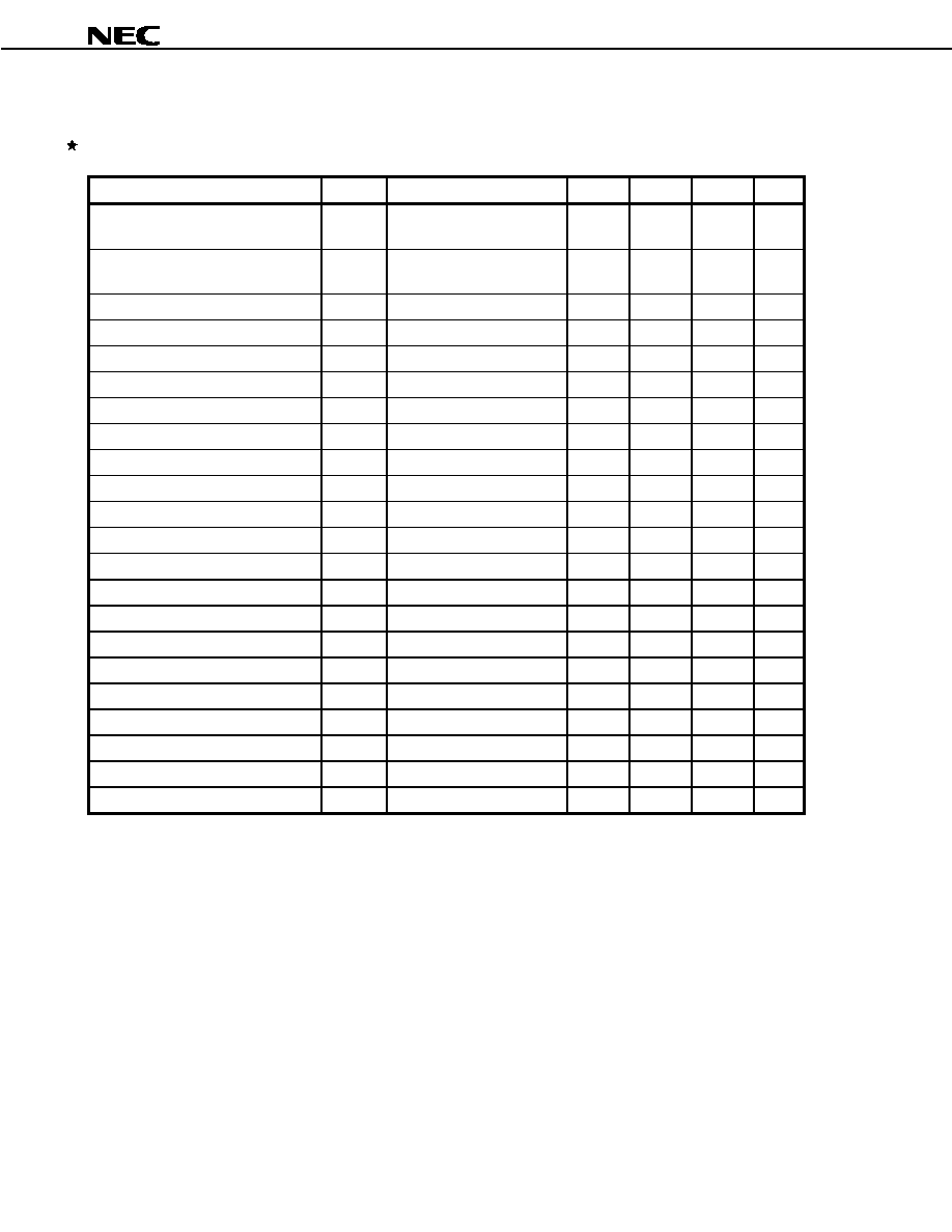
2. ELECTRICAL SPECIFICATIONS
* indicates changes from the Preliminary Data Sheet (document number: S12689E, 1st edition).
Absolute Maximum Ratings
Parameter
Symbol
Condition
Rating
Unit
V
DD
¡0.5 to +4.6
V
Supply voltage
V
DD5
Note 1
¡0.5 to +6.5
V
Normal I/O pin
¡0.5 to +6.6
V
*
PCI I/O pin
Note 2
¡0.5 to +6.6
V
*
Input/output voltage
V
I
/V
O
P-ECL pin
¡0.5 to +4.6 and V
DD
+ 0.5
V
*
Ambient operating frequency
T
A
0 to +70
░C
Storage temperature
T
stg
¡65 to +150
░C
Notes 1. V
DD5
: Clamping diode-dedicated power supply
2. By supplying 5 V for clamping diode, the device can be protected from an 11-V reflection wave.
Caution If any of the parameters exceeds the absolute maximum ratings, even momentarily, the quality of
the product may be impaired. The absolute maximum ratings are values that may physically
damage the product(s). Be sure to use the product(s) within the ratings.
Recommended Operating Conditions
Parameter
Symbol
Condition
MIN.
TYP.
MAX.
Unit
V
DD
+3.0
+3.3
+3.6
V
V
DD5
Note
+3.3 V PCI
+3.0
+3.3
+3.6
V
Supply voltage
V
DD5
Note
+5 V PCI
+4.75
+5.00
+5.25
V
Ambient operating temperature
T
A
0
+70
░C
V
IH1
Input pins other than PCI
and P-ECL
+2.0
+5.5
V
V
IH2
+5-V PCI pin
+2.0
V
DD5
+ 0.5
V
*
V
IH3
+3.3-V PCI pin
0.5
Î
V
DD
V
DD
+ 0.5
V
*
High-level input voltage
V
IH4
P-ECL pin
V
DD
¡ 1.49
V
DD
¡ 0.40
V
*
V
IL1
Input pins other than PCI
and P-ECL
0
+0.8
V
V
IL2
+5-V PCI pin
¡0.5
+0.8
V
V
IL3
+3.3-V PCI pin
¡0.5
0.3
Î
V
DD
V
Low-level input voltage
V
IL4
P-ECL pin
V
DD
¡ 2.82
V
DD
¡ 1.50
V
*
Note V
DD5
: Clamping diode-dedicated power supply
Data Sheet S12689EJ2V0DS00
26
Á
Á
Á
Á
PD98405
DC Characteristics (T
A
= 0 to +70░C, V
DD
= +3.3 V
▒
▒
▒
▒
0.3 V)
Parameter
Symbol
Condition
MIN.
TYP.
MAX.
Unit
V
OH1
I
OH
= ¡3.0 mA
Note 1
+2.4
V
V
OH2
I
OH
= ¡500
Á
A
Note 2
(+3.3 V PCI)
0.88
Î
V
DD
V
*
V
OH3
I
OH
= ¡2.0 mA
Note 2
(+5 V PCI)
+2.4
V
High-level output voltage
V
OH4
R
L
= 50
, V
T
= V
DD
¡ 2 V
(P-ECL)
V
DD
¡ 1.140
V
DD
¡ 0.690
V
*
V
OL1
I
OL
= 9.0 mA
Note 1
0.144
Î
V
DD
V
*
V
OL2
I
OL
= 1500
Á
A
Note 2
(+3.3 V PCI)
+0.4
V
V
OL3
I
OL
= 3.0 mA
Note 2
(+5 V PCI)
+0.55
V
V
OL4
I
OL
= 6.0 mA
Note 4
(+5 V PCI)
+0.55
V
Low-level output voltage
V
OL5
R
L
= 50
, V
T
= V
DD
¡ 2 V
(P-ECL)
V
DD
¡ 2.175
V
DD
¡ 1.755
V
*
Supply current
I
DD
f
CLK
= 33 MHz, normal operation
650
900
mA
*
Input leakage current (normal input)
I
I1
V
I
= V
DD
▒
10
Á
A
*
Input leakage current
Note 5
I
I2
V
I
= V
DD
or GND
28
160
Á
A
*
Notes 1. V
OH1
and V
OL1
are applied to the following pins (output pins other than PCI):
CD31-CD0, CPAR3-CPAR0, CA18-CA0, CBE3_B-CBE0_B, CWE_B, COE_B, JDO, RCLK, RENBL_B,
TSOC, TENBL_B, TCLK, Tx7-Tx0, PHCE_B, PHOE_B, PHRW_B, E2PCS, E2PDO, E2PCLK
2. V
OH2
, V
OH3
, and V
OL2
are applied to the following pins (PCI output pins):
AD63-AD0, PCBE7_B-PCBE0_B, PAR, PAR64, REQ_B, INTR_B, FRAME_B, REQ64_B, TRDY_B,
IRDY_B, DEVSEL_B, STOP_B, SERR_B, PERR_B
3. V
OL3
is applied to the following pins (with +5-V PCI):
AD31-AD0, PCBE3_B-PCBE0_B, PAR, REQ_B, INTR_B
4. V
OL4
is applied to the following pins (with +5-V PCI):
FRAME_B, TRDY_B, IRDY_B, DEVSEL_B, STOP_B, SERR_B, PERR_B, AD64-AD32, PCBE7_B-
PCBE4_B, ACK64_B, REQ64_B, PAR64
5. I
I2
is applied to the following pins:
E2PDI, ROMD7-ROMD0, FULL_B, EMPTY_B, RSOC, Rx7-Rx0, CPAR3-CPAR0, CD31-CD0,
PCI_MODE
Data Sheet S12689EJ2V0DS00
27
Á
Á
Á
Á
PD98405
Capacitance (T
A
= +25░C, V
DD
= 0 V)
Parameter
Symbol
Condition
MIN.
TYP.
MAX.
Unit
Input capacitance
C
IN
10
pF
CLK input capacitance
C
CLK
5
12
pF
IDSEL input capacitance
C
IDSEL
8
pF
Output capacitance
C
OUT
8
10
pF
I/O capacitance
C
I/O
8
pF
Internal pull-down resistor (T
A
= 0 to +70░C, V
DD
= +3.3 V
▒
▒
▒
▒
0.3 V)
Parameter
Symbol
Condition
MIN.
TYP.
MAX.
Unit
Internal pull-down resistance
R
PD
E2PDI, ROMD7-ROMD0,
RSOC, Rx7-Rx2, CPAR3-
CPAR0, CD31-CD0,
PCI_MODE
21.8
37.1
83.1
k
*
Data Sheet S12689EJ2V0DS00
28
Á
Á
Á
Á
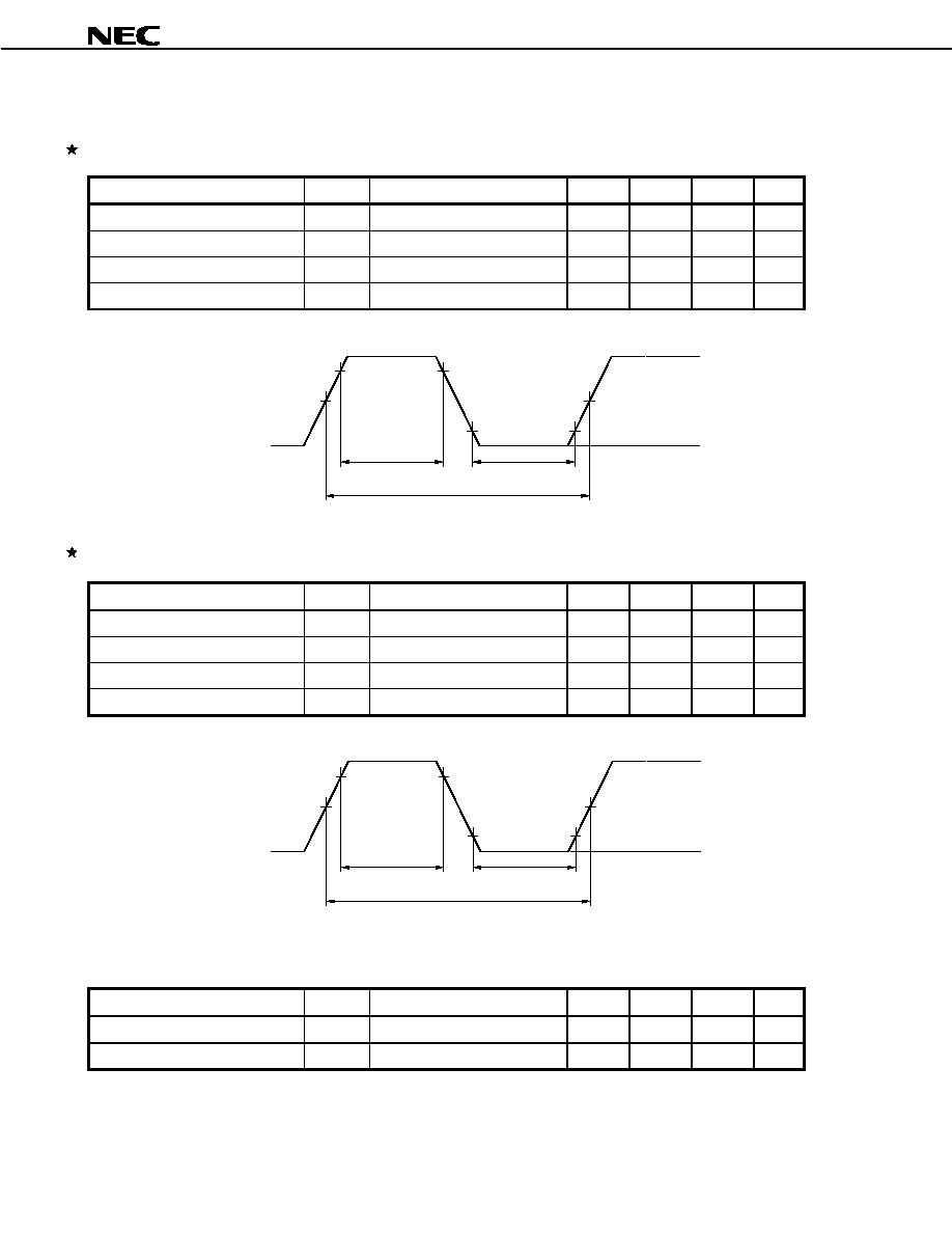
PD98405
AC Characteristics (T
A
= 0 to +70░C, V
DD
= +3.3 V
▒
▒
▒
▒
0.3 V, output pin load: 30 pF)
CLK input (BUS interface clock - CLK pin)
Parameter
Symbol
Condition
MIN.
TYP.
MAX.
Unit
CLK cycle time
t
CYCLK
30
125
ns
CLK high-level width
t
CLKH
11
ns
CLK low-level width
t
CLKL
11
ns
CLK slew rate
slew
CLK
1
4
V/ns
t
CLKH
t
CLKL
t
CYCLK
2.0 V
1.5 V
0.8 V
2.4 V (MIN.)
0.4 V (MAX.)
CLK
SCLK input (internal system clock - SCLK pin)
Parameter
Symbol
Condition
MIN.
TYP.
MAX.
Unit
SCLK cycle time
t
CYSCLK
40
125
ns
SCLK high-level width
t
SCLKH
15
ns
SCLK low-level width
t
SCLKL
15
ns
SCLK slew rate
slew
SCLK
1
4
V/ns
t
SCLKH
t
SCLKL
t
CYSCLK
2.0 V
1.5 V
0.8 V
2.4 V (MIN.)
0.4 V (MAX.)
SCLK
RST input
Parameter
Symbol
Condition
MIN.
TYP.
MAX.
Unit
RST low-level width
t
RSTL
t
CYCLK
ns
RST slew rate
slew
RST
50
V/ns

Data Sheet S12689EJ2V0DS00
29
Á
Á
Á
Á
PD98405
[MEMO]
Data Sheet S12689EJ2V0DS00
30
Á
Á
Á
Á
PD98405
PCI Bus Interface
Bus master read
Parameter
Symbol
Condition
MIN.
TYP.
MAX.
Unit
CLK
FRAME_B, REQ64_B valid
time
t
DFRAME
1
11
ns
*
CLK
FRAME_B, REQ64_B float
time
t
DFRAMEF
28
ns
*
CLK
AD (Address) valid time
t
DADDR
1
11
ns
*
CLK
AD (Address) float time
t
DADDRF
28
ns
AD (Data) setup time
t
SDATA
8
ns
*
AD (Data) hold time
t
HDATA
1
ns
*
CLK
PCBE_B valid time
t
DPCBE
1
11
ns
*
CLK
PCBE_B float time
t
DPCBEF
28
ns
CLK
IRDY_B valid time
t
DIRDY
1
11
ns
*
CLK
IRDY_B float time
t
DIRDYF
28
ns
*
TRDY_B setup time
t
STRDY
8
ns
*
TRDY_B hold time
t
HTRDY
1
ns
*
DEVSEL_B, ACK64_B setup time
t
SDEVSEL
8
ns
*
DEVSEL_B, ACK64_B hold time
t
HDEVSEL
1
ns
*
STOP_B setup time
t
SSTOP
8
ns
*
STOP_B hold time
t
HSTOP
1
ns
*
CLK
PAR valid time
t
DPAR
1
11
ns
*
CLK
PAR float time
t
DPARF
28
ns
PAR setup time
t
SPAR
8
ns
*
PAR hold time
t
HPAR
1
ns
*
CLK
PERR_B valid time
t
DPERR
1
11
ns
*
CLK
PERR_B float time
t
DPERRF
28
ns
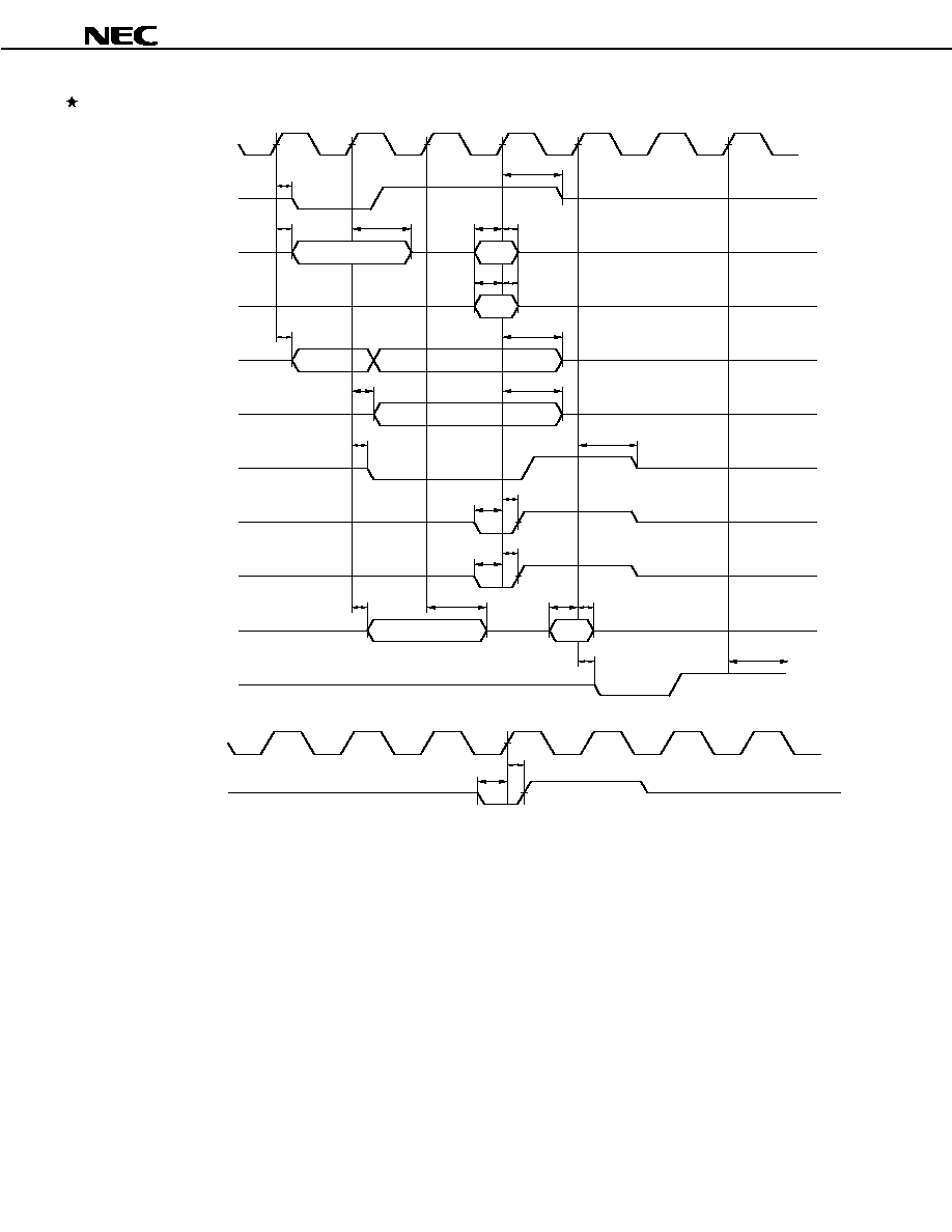
Data Sheet S12689EJ2V0DS00
31
Á
Á
Á
Á
PD98405
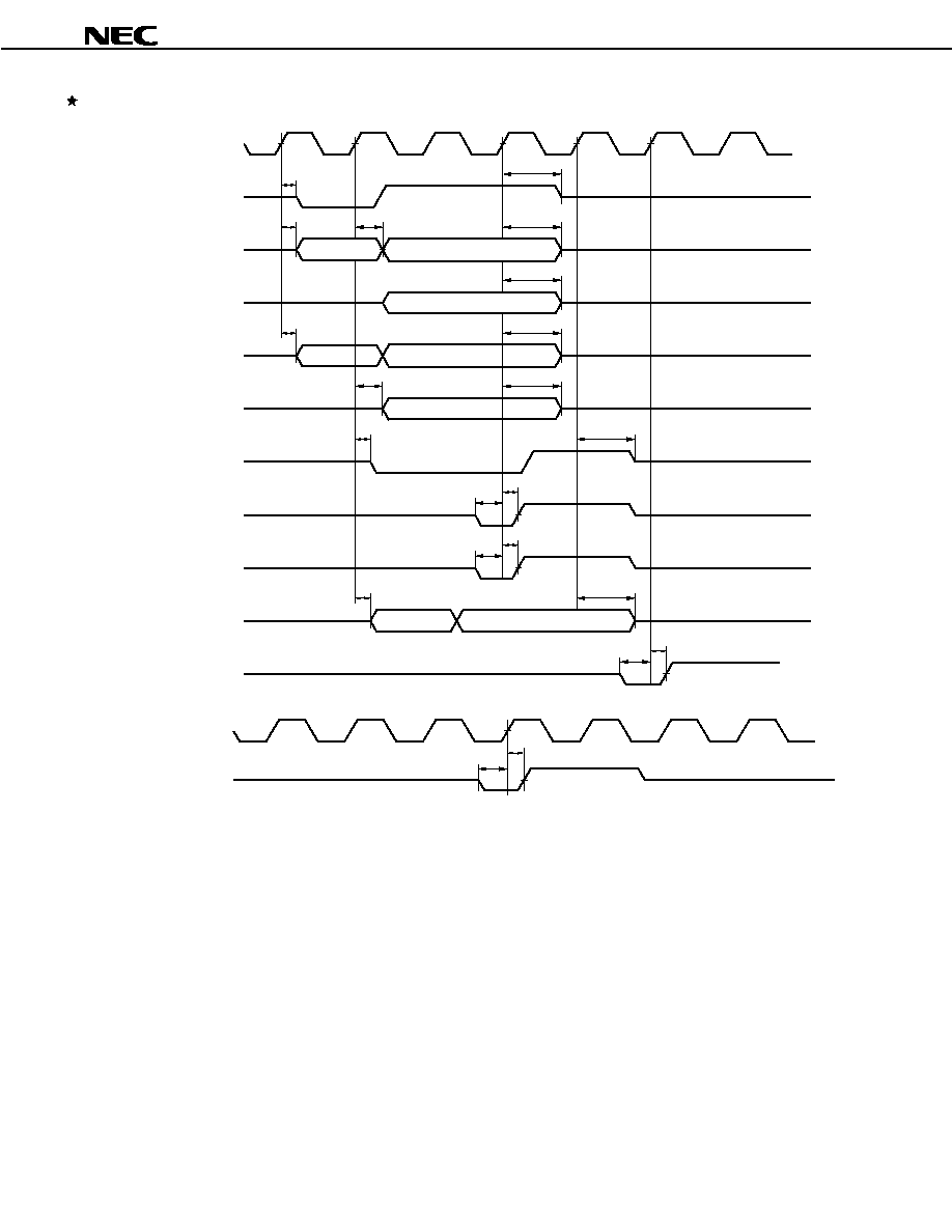
Bus master read
CLK
FRAME_B
REQ64_B
AD31-AD0
AD63-AD32
IRDY_B
TRDY_B
PERR_B
CLK
STOP_B
PCBE3_B-
PCBE0_B
PCBE7_B-
PCBE4_B
DEVSEL_B
ACK64_B
PAR
PAR64
(Address)
(Data)
(Data)
t
HTRDY
t
STRDY
t
HDEVSEL
t
SDEVSEL
t
DFRAME
t
DFRAMEF
t
DADDRF
t
DADDR
t
SDATA
t
HDATA
t
SDATA
t
HDATA
t
DPCBE
t
DPCBEF
t
DPCBEF
t
DPCBE
t
DIRDY
t
DIRDYF
(Output)
(Input)
t
DPARF
t
DPAR
t
SPAR
t
HPAR
t
DPERR
t
DPERRF
t
HSTOP
t
SSTOP
Data Sheet S12689EJ2V0DS00
32
Á
Á
Á
Á
PD98405
Bus master write
Parameter
Symbol
Condition
MIN.
TYP.
MAX.
Unit
CLK
FRAME_B, REQ64_B valid
time
t
DFRAME
1
11
ns
*
CLK
FRAME_B, REQ64_B float
time
t
DFRAMEF
28
ns
*
CLK
AD (Address) valid time
t
DADDR
1
11
ns
*
CLK
Data valid time
t
DDATA
1
11
ns
*
CLK
Data float time
t
DDATAF
28
ns
CLK
PCBE_B valid time
t
DPCBE
1
11
ns
*
CLK
PCBE_B float time
t
DPCBEF
28
ns
CLK
IRDY_B valid time
t
DIRDY
1
11
ns
*
CLK
IRDY_B float time
t
DIRDYF
28
ns
TRDY_B setup time
t
STRDY
8
ns
*
TRDY_B hold time
t
HTRDY
1
ns
*
STOP_B setup time
t
SSTOP
8
ns
*
STOP_B hold time
t
HSTOP
1
ns
*
DEVSEL_B, ACK64_B setup time
t
SDEVSEL
8
ns
*
DEVSEL_B, ACK64_B hold time
t
HDEVSEL
1
ns
*
CLK
PAR valid time
t
DPAR
1
11
ns
*
CLK
PAR float time
t
DPARF
28
ns
PERR_B setup time
t
SPERR
8
ns
*
PERR_B hold time
t
HPERR
1
ns
*
Data Sheet S12689EJ2V0DS00
33
Á
Á
Á
Á
PD98405
Bus master write
CLK
FRAME_B
REQ64_B
AD31-AD0
AD63-AD32
IRDY_B
TRDY_B
PERR_B
CLK
STOP_B
PCBE3_B-
PCBE0_B
PCBE7_B-
PCBE4_B
DEVSEL_B
ACK64_B
PAR
PAR64
(Data)
t
HTRDY
t
STRDY
t
HDEVSEL
t
SDEVSEL
t
DFRAME
t
DFRAMF
t
DPCBE
t
DPCBEF
t
DPCBEF
t
DPCBE
t
DIRDY
t
DIRDYF
t
DPARF
t
DPAR
t
HSTOP
t
SSTOP
t
DADDR
t
DDATAF
t
DDATA
(Address)
(Data)
t
DDATAF
(Output)
(Output)
t
SPERR
t
HPERR
Data Sheet S12689EJ2V0DS00
34
Á
Á
Á
Á
PD98405
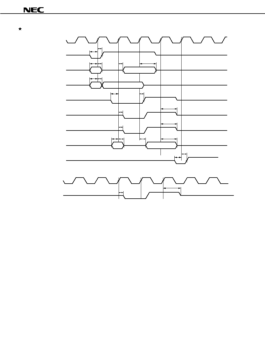
Target read
Parameter
Symbol
Condition
MIN.
TYP.
MAX.
Unit
FRAME_B setup time
t
SFRAME
8
ns
*
FRAME_B hold time
t
HFRAME
1
ns
*
AD (Address) setup time
t
SADDR
8
ns
*
AD (Address) hold time
t
HADDR
1
ns
*
CLK
AD (Data) valid time
t
DDATA
1
11
ns
*
CLK
AD (Data) float time
t
DDATAF
28
ns
PCBE_B setup time
t
SPCBE
8
ns
*
PCBE_B hold time
t
HPCBE
1
ns
*
IRDY_B setup time
t
SIRDY
8
ns
*
IRDY_B hold time
t
HIRDY
1
ns
*
CLK
TRDY_B valid time
t
DTRDY
1
11
ns
*
CLK
TRDY_B float time
t
DTRDYF
28
ns
CLK
STOP_B valid time
t
DSTOP
1
11
ns
*
CLK
STOP_B float time
t
DSTOPF
28
ns
*
CLK
DEVSEL_B valid time
t
DDEVSEL
1
11
ns
*
CLK
DEVSEL_B float time
t
DDEVSELF
28
ns
PAR setup time
t
SPAR
8
ns
*
PAR hold time
t
HPAR
1
ns
*
CLK
PAR valid time
t
DPAR
1
11
ns
*
CLK
PAR float time
t
DPARF
28
ns
PERR_B setup time
t
SPERR
8
ns
*
PERR_B hold time
t
HPERR
1
ns
*
Data Sheet S12689EJ2V0DS00
35
Á
Á
Á
Á
PD98405
Target read
CLK
FRAME_B
AD31-AD0
IRDY_B
TRDY_B
PERR_B
CLK
STOP_B
PCBE3_B-
PCBE0_B
DEVSEL_B
PAR
(Address)
(Data)
t
DTRDY
t
SFRAME
t
HFRAME
t
HADDR
t
SIRDY
t
DTRDYF
(Input)
(Output)
t
SPAR
t
HPERR
t
DSTOPF
t
DSTOP
t
SADDR
t
DDATA
t
DDATAF
t
HPCBE
t
SPCBE
t
HIRDY
t
DDEVSEL
t
DDEVSELF
t
DPAR
t
DPARF
t
HPAR
t
SPERR
Data Sheet S12689EJ2V0DS00
36
Á
Á
Á
Á
PD98405
Target write
Parameter
Symbol
Condition
MIN.
TYP.
MAX.
Unit
FRAME_B setup time
t
SFRAME
8
ns
*
FRAME_B hold time
t
HFRAME
1
ns
*
AD (Address) setup time
t
SADDR
8
ns
*
AD (Address) hold time
t
HADDR
1
ns
*
AD (Data) setup time
t
SDATA
8
ns
*
AD (Data) hold time
t
HDATA
1
ns
*
PCBE_B setup time
t
SPCBE
8
ns
*
PCBE_B hold time
t
HPCBE
1
ns
*
IRDY_B setup time
t
SIRDY
8
ns
*
IRDY_B hold time
t
HIRDY
1
ns
*
CLK
TRDY_B valid time
t
DTRDY
1
11
ns
*
CLK
TRDY_B float time
t
DTRDYF
28
ns
CLK
STOP_B valid time
t
DSTOP
1
11
ns
*
CLK
STOP_B float time
t
DSTOPF
28
ns
*
CLK
DEVSEL_B valid time
t
DDEVSEL
1
11
ns
*
CLK
DEVSEL_B float time
t
DDEVSELF
28
ns
PAR setup time
t
SPAR
8
ns
*
PAR hold time
t
HPAR
1
ns
*
CLK
PERR_B valid time
t
DPERR
1
11
ns
*
CLK
PERR_B float time
t
DPERRF
28
ns
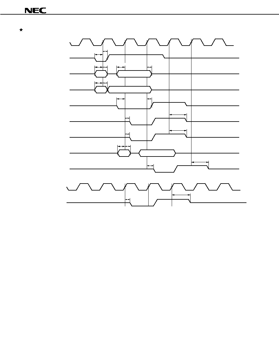
Data Sheet S12689EJ2V0DS00
37
Á
Á
Á
Á
PD98405
Target write
CLK
FRAME_B
AD31-AD0
IRDY_B
TRDY_B
PERR_B
CLK
STOP_B
PCBE3_B-
PCBE0_B
DEVSEL_B
PAR
(Address)
(Data)
t
DTRDY
t
SFRAME
t
HFRAME
t
HADDR
t
HDATA
t
SIRDY
t
DTRDYF
(Input)
(Input)
t
SPAR
t
DSTOPF
t
DSTOP
t
SADDR
t
HPCBE
t
SPCBE
t
HIRDY
t
DDEVSEL
t
DDEVSELF
t
HPAR
t
SDATA
t
DPERR
t
DPERRF
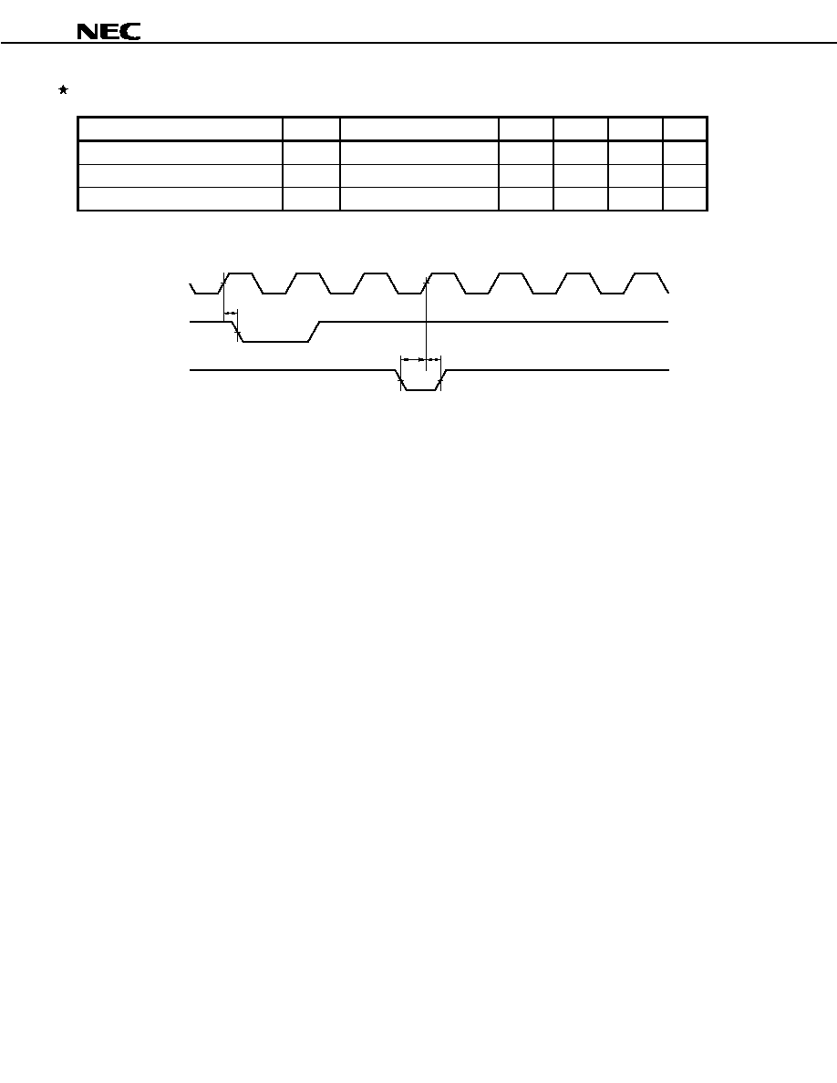
Data Sheet S12689EJ2V0DS00
38
Á
Á
Á
Á
PD98405
Bus arbitration
Parameter
Symbol
Condition
MIN.
TYP.
MAX.
Unit
CLK
REQ_B valid time
t
DREQ
1
12
ns
*
GNT_B setup time
t
SGNT
10
ns
GNT_B hold time
t
HGNT
1
ns
*
Bus arbitration
CLK
REQ_B
GNT_B
t
DREQ
t
SGNT
t
HGNT
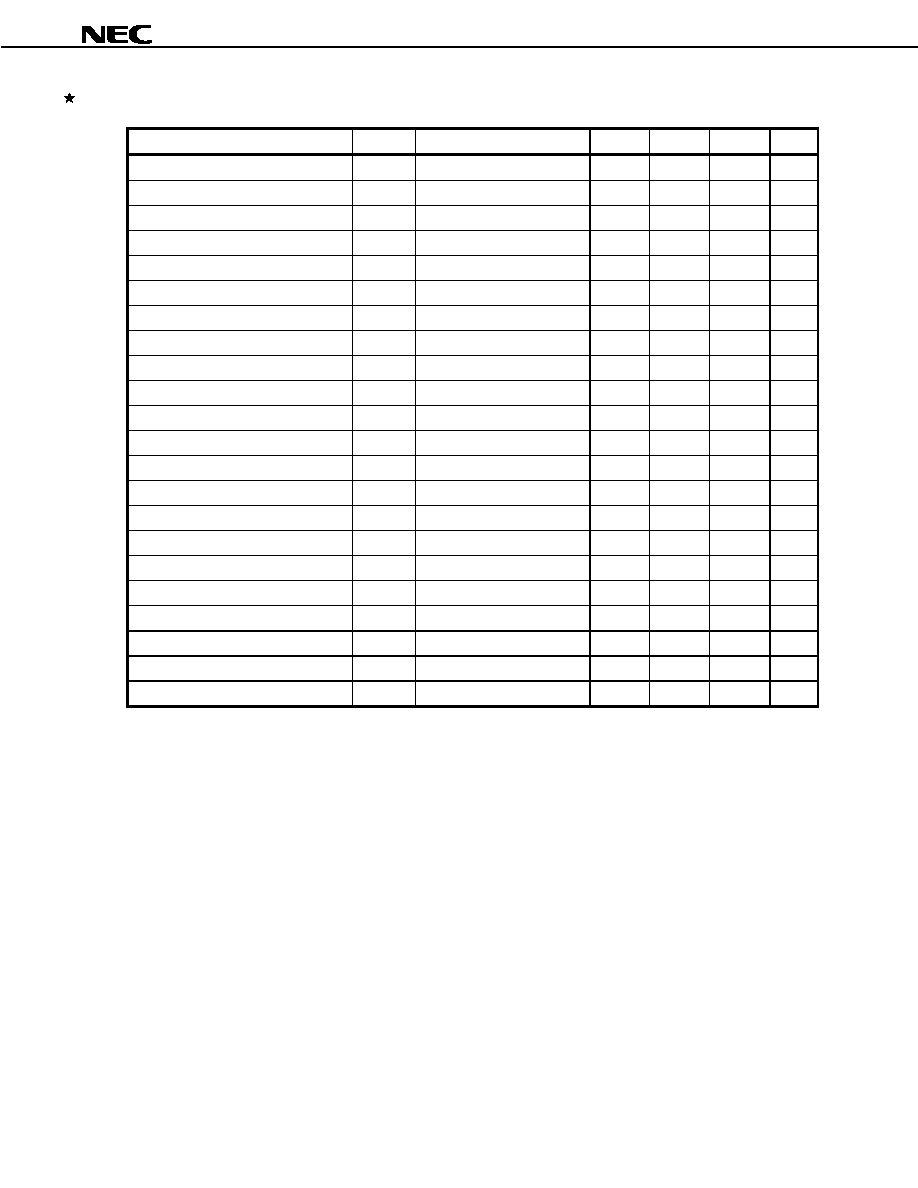
Data Sheet S12689EJ2V0DS00
39
Á
Á
Á
Á
PD98405
Configuration read
Parameter
Symbol
Condition
MIN.
TYP.
MAX.
Unit
FRAME_B setup time
t
SFRAME
8
ns
*
FRAME_B hold time
t
HFRAME
1
ns
*
AD (Address) setup time
t
SADDR
8
ns
*
AD (Address) hold time
t
HADDR
1
ns
*
CLK
AD (Data) valid time
t
DDATA
1
11
ns
*
CLK
AD (Data) float time
t
DDATAF
28
ns
PCBE_B setup time
t
SPCBE
8
ns
*
PCBE_B hold time
t
HPCBE
1
ns
*
IDSEL setup time
t
SIDSEL
8
ns
*
IDSEL hold time
t
HIDSEL
1
ns
*
IRDY_B setup time
t
SIRDY
8
ns
*
IRDY_B hold time
t
HIRDY
1
ns
*
CLK
TRDY_B valid time
t
DTRDY
1
11
ns
*
CLK
TRDY_B float time
t
DTRDYF
28
ns
CLK
DEVSEL_B valid time
t
DDEVSEL
1
11
ns
*
CLK
DEVSEL_B float time
t
DDEVSELF
28
ns
CLK
PAR valid time
t
DPAR
1
11
ns
*
CLK
PAR float time
t
DPARF
28
ns
PAR setup time
t
SPAR
8
ns
*
PAR hold time
t
HPAR
1
ns
*
PERR_B setup time
t
SPERR
8
ns
*
PERR_B hold time
t
HPERR
1
ns
*
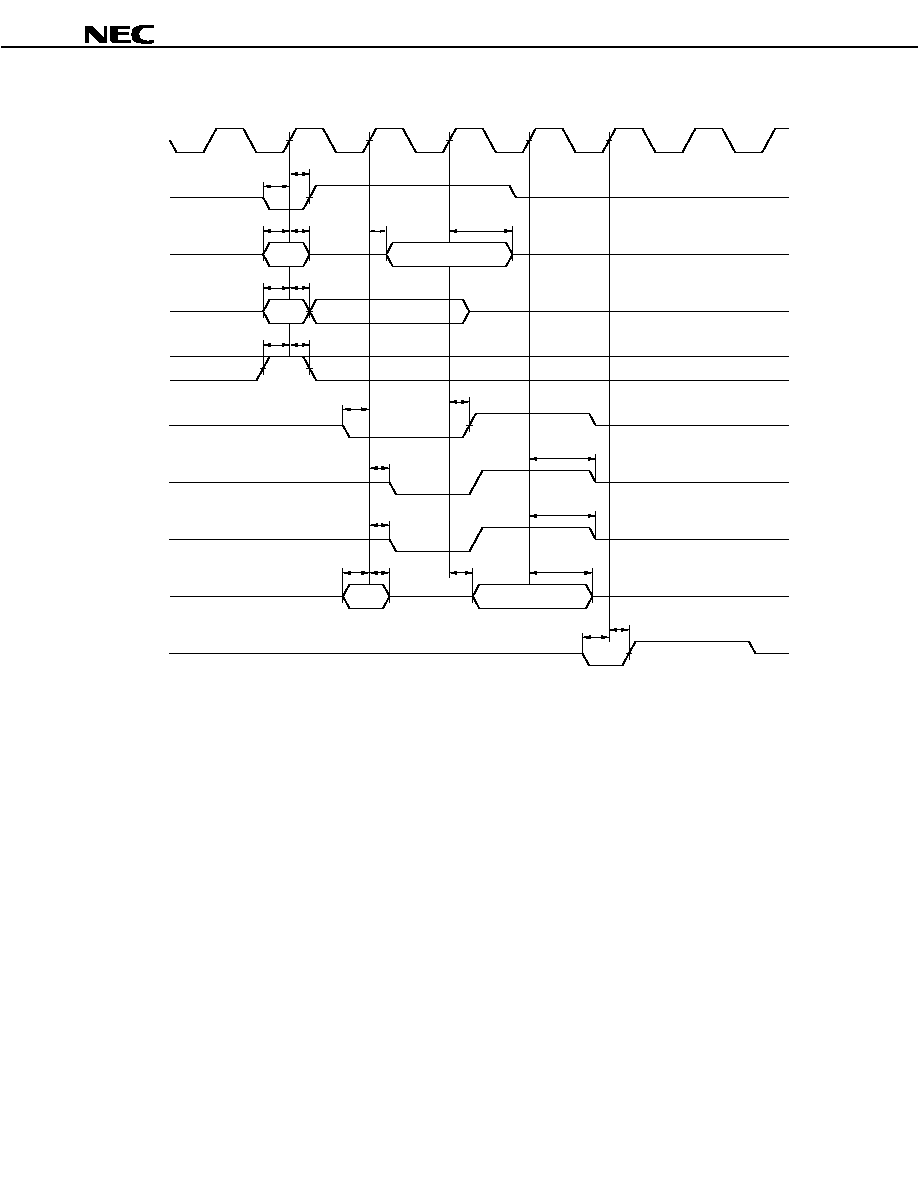
Data Sheet S12689EJ2V0DS00
40
Á
Á
Á
Á
PD98405
Configuration read
CLK
FRAME_B
AD31-AD0
PCBE3_B-
PCBE0_B
IDSEL
IRDY_B
TRDY_B
DEVSEL_B
PAR
PERR_B
(Address)
(Data)
t
SIRDY
t
HIRDY
t
DTRDY
t
DTRDYF
t
DDEVSEL
t
DDEVSELF
t
SADDR
t
HADDR
t
DDATA
t
DDATAF
(Input)
(Output)
t
SPAR
t
HPAR
t
DPAR
t
DPARF
t
SPERR
t
HPERR
t
SFRAME
t
HFRAME
t
SPCBE
t
HPCBE
t
SIDSEL
t
HIDSEL
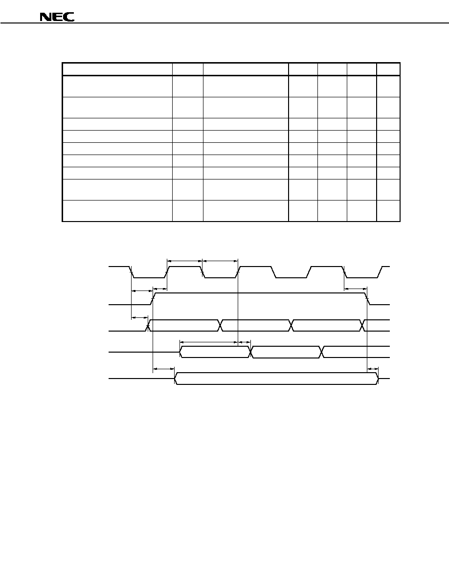
Data Sheet S12689EJ2V0DS00
41
Á
Á
Á
Á
PD98405
EEPROM interface
Parameter
Symbol
Condition
MIN.
TYP.
MAX.
Unit
E2PCLK high-level width
t
WE2PCKLH
t
CYCLK
Î
18
¡ 50
t
CYCLK
Î
18 t
CYCLK
Î
18
+ 50
ns
E2PCLK low-level width
t
WE2PCLKL
t
CYCLK
Î
18
¡ 50
t
CYCLK
Î
18 t
CYCLK
Î
18
+ 50
ns
E2PCLK
E2PCS valid time
t
DE2PCS
50
ns
E2PCS
E2PCLK
t
SE2PCS
50
ns
E2PCLK
E2PDO valid time
t
DE2PDO
300
ns
E2PDI
E2PCLK setup time
t
SE2PDI
500
ns
E2PCLK
E2PDI hold time
t
HE2PDI
70
ns
E2PCS
E2PDI (Status) valid
delay time
t
DE2PSTV
500
ns
E2PCS
E2PDI (Status) invalid
delay time
t
DE2PSTI
0
100
ns
EEPROM interface
E2PCLK
E2PCS
E2PDO
E2PDI
(READ)
E2PDI
(Status)
t
WE2PCLKH
t
WE2PCLKL
t
DE2PCS
t
SE2PCS
t
DE2PDO
t
SE2PDI
t
HE2PDI
t
DE2PSTV
t
DE2PSTI
t
DE2PCS
(Status)
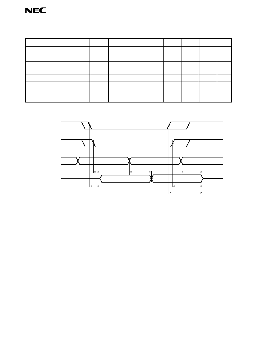
Data Sheet S12689EJ2V0DS00
42
Á
Á
Á
Á
PD98405
Expansion ROM interface
Parameter
Symbol
Condition
MIN.
TYP.
MAX.
Unit
ROMOE_B
ROMD valid time
t
DROMOE
ROMCS_B = V
OL
, ROMA valid
200
ns
ROMCS_B
ROMD valid time
t
DROMCS
ROMOE_B = V
OL
, ROMA valid
200
ns
ROMA valid time
ROMD valid
time
t
ROMACC
ROMCS_B = ROMOE_B = V
OL
200
ns
ROMOE_B
ROMD float time
t
HROMOE
ROMCS_B = V
OL
, ROMA valid
0
ns
ROMCS_B
ROMD float time
t
HROMCS
ROMOE_B = V
OL
, ROMA valid
0
ns
ROMA invalid time
ROMD hold
time
t
HROMA
ROMCS_B = ROMOE_B = V
OL
0
ns
Expansion ROM interface
ROMA15-
ROMA0
ROMCS_B
ROMOE_B
ROMD7-
ROMD0
t
DROMCS
t
DROMOE
t
ROMACC
t
HROMA
t
HROMOE
t
HROMCS
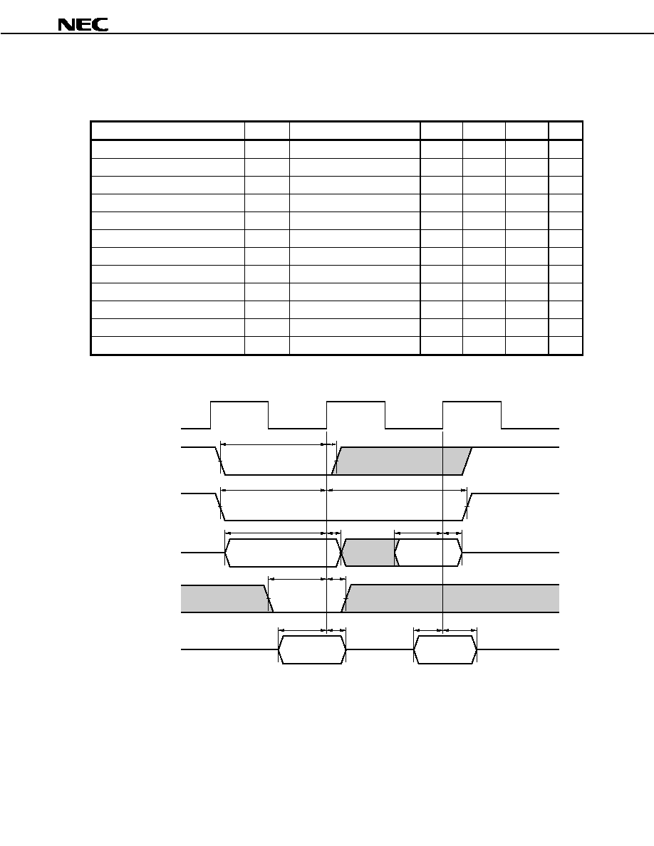
Data Sheet S12689EJ2V0DS00
43
Á
Á
Á
Á
PD98405
Generic bus interface
Slave write access
Parameter
Symbol
Condition
MIN.
TYP.
MAX.
Unit
ASEL_B setup time
t
SASEL
8
ns
ASEL_B hold time
t
HASEL
3
ns
SEL_B setup time
t
SSEL
8
ns
SEL_B hold time
t
HSEL
1 t
CYCLK
+ 3
ns
Address setup time
t
SDADD
8
ns
Address hold time
t
HDADD
3
ns
Data setup time
t
SDDAT
8
ns
Data hold time
t
HDDAT
3
ns
PAR setup time
t
SPAR1
8
ns
PAR hold time
t
HPAR1
3
ns
SR/W_B setup time
t
SSRW
8
ns
SR/W_B hold time
t
HSRW
3
ns
Slave write access
CLK
ASEL_B
SEL_B
AD31-AD0
SR/W_B
PAR3-PAR0
t
SASEL
t
HASEL
t
SSEL
t
HSEL
t
SDADD
t
HDADD
t
SDDAT
t
HDDAT
t
SSRW
t
HSRW
t
SPAR1
t
HPAR1
(Input)
t
SPAR1
t
HPAR1
(Input)
Address
Data
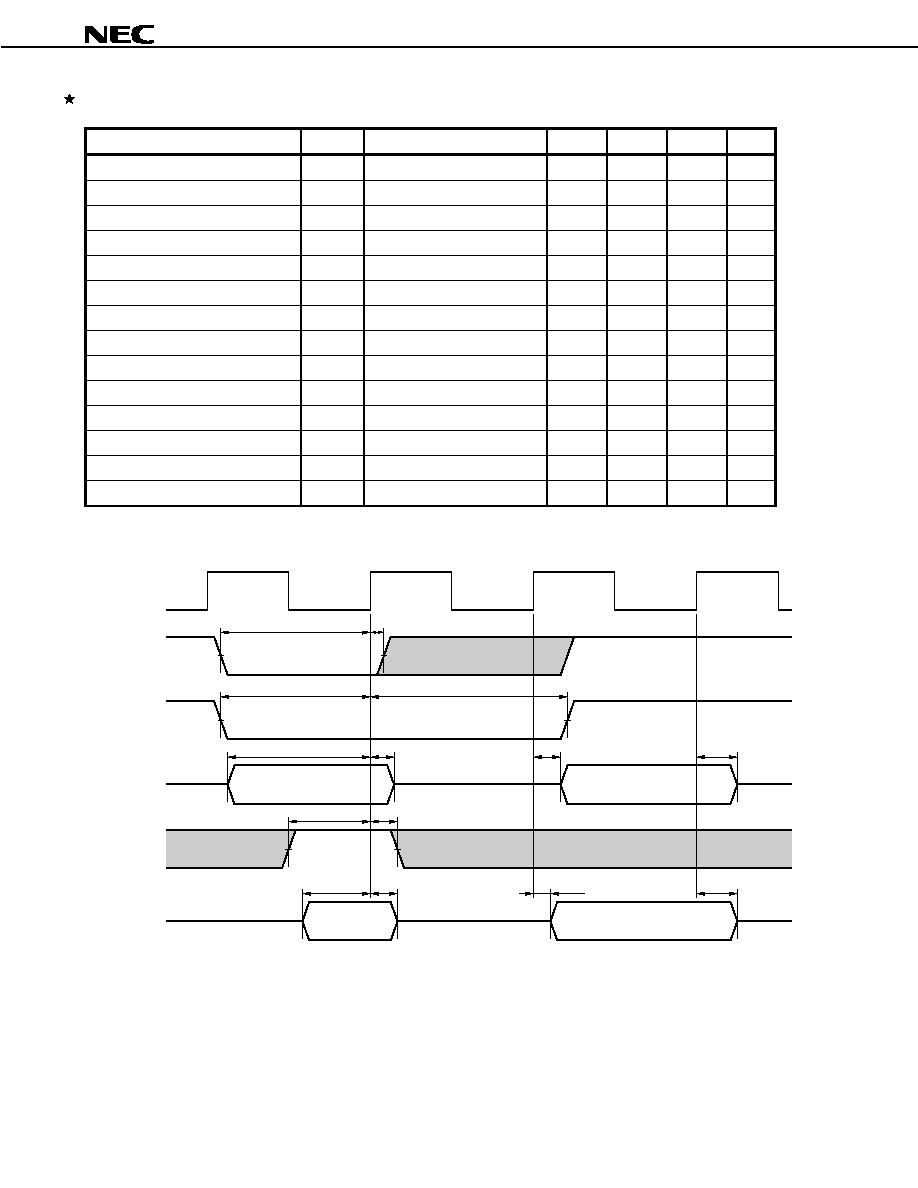
Data Sheet S12689EJ2V0DS00
44
Á
Á
Á
Á
PD98405
Slave read access
Parameter
Symbol
Condition
MIN.
TYP.
MAX.
Unit
ASEL_B setup time
t
SASEL
8
ns
ASEL_B hold time
t
HASEL
3
ns
SEL_B setup time
t
SSEL
8
ns
SEL_B hold time
t
HSEL
1 t
CYCLK
+ 3
ns
Address setup time
t
SDADD
8
ns
Address hold time
t
HDADD
3
ns
CLK
data delay time
t
DDDAT
18
ns
CLK
data float time
t
FDDAT
2
18
ns
*
PAR setup time
t
SPAR1
8
ns
PAR hold time
t
HPAR1
3
ns
CLK
PAR delay time
t
DPAR1
18
ns
CLK
PAR float time
t
FPAR1
2
18
ns
*
SR/W_B setup time
t
SSRW
8
ns
SR/W_B hold time
t
HSRW
3
ns
Slave read access
CLK
ASEL_B
SEL_B
AD31-AD0
SR/W_B
PAR3-PAR0
t
SASEL
t
HASEL
t
SSEL
t
HSEL
t
SDADD
t
HDADD
t
DDDAT
t
SSRW
t
HSRW
t
SPAR1
t
HPAR1
(Input)
t
DPAR1
t
FPAR1
(Output)
Address (input)
Data (output)
t
FDDAT
Data Sheet S12689EJ2V0DS00
45
Á
Á
Á
Á
PD98405
DMA write access
Parameter
Symbol
Condition
MIN.
TYP.
MAX.
Unit
CLK
ATTN_B delay time
t
DATTN
18
ns
GNT_B setup time
t
SGNT
8
ns
GNT_B hold time
t
HGNT
3
ns
CLK
DR/W_B delay time
t
DDRW
2
18
ns
*
CLK
SIZE delay time
t
DSIZE
2
18
ns
*
CLK
address delay time
t
DSADD
18
ns
CLK
address/data float time
t
FSADD
2
18
ns
*
CLK
BE_B delay time
t
DSBE
18
ns
CLK
BE_B float time
t
FSBE
2
18
ns
*
CLK
PAR delay time
t
DPAR2
18
ns
CLK
PAR float time
t
FPAR2
2
18
ns
*
RDY_B setup time
t
SRDY
8
ns
RDY_B hold time
t
HRDY
3
ns
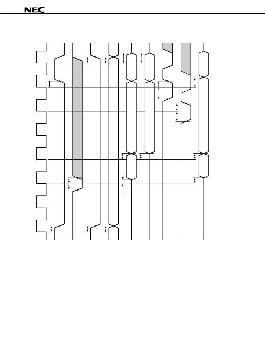
D
a
ta S
heet S
12689E
J2V
0
D
S
00
46
Á
Á
Á
Á
P
D
98405
CLK
ATTN_B
GNT_B
DR/W_B
SIZE2-SIZE0
AD31-AD0
BE3_B-BE0_B
RDY_B
(Normal mode)
RDY_B
(Early mode)
PAR3-PAR0
Address (output)
Data 0 (output)
Data 1 (output)
BE 0 (output)
BE 1 (output)
(Output)
(Output)
(Output)
t
DATTN
t
HGNT
t
SGNT
t
DATTN
t
DDRW
t
DSIZE
t
DSADD
t
FSADD
t
DSBE
t
DDRW
t
DSIZE
t
FSADD
t
FSBE
t
HRDY
t
SRDY
t
HRDY
t
SRDY
t
DPAR2
t
FPAR2
t
DPAR2
DMA write access (Example: 2-word burst)
Data Sheet S12689EJ2V0DS00
47
Á
Á
Á
Á
PD98405
DMA read access
Parameter
Symbol
Condition
MIN.
TYP.
MAX.
Unit
CLK
ATTN_B delay time
t
DATTN
18
ns
GNT_B setup time
t
SGNT
8
ns
GNT_B hold time
t
HGNT
3
ns
CLK
DR/W_B delay time
t
DDRW
2
18
ns
*
CLK
SIZE delay time
t
DSIZE
2
18
ns
*
CLK
address delay time
t
DSADD
18
ns
CLK
address/data float time
t
FSADD
2
18
ns
*
CLK
BE_B delay time
t
DSBE
18
ns
CLK
BE_B float time
t
FSBE
2
18
ns
*
CLK
PAR delay time
t
DPAR2
18
ns
RDY_B setup time
t
SRDY
8
ns
RDY_B hold time
t
HRDY
3
ns
Data setup time
t
SSDAT
8
ns
Data hold time
t
HSDAT
3
ns
PAR setup time
t
SPAR2
8
ns
PAR hold time
t
HPAR2
3
ns
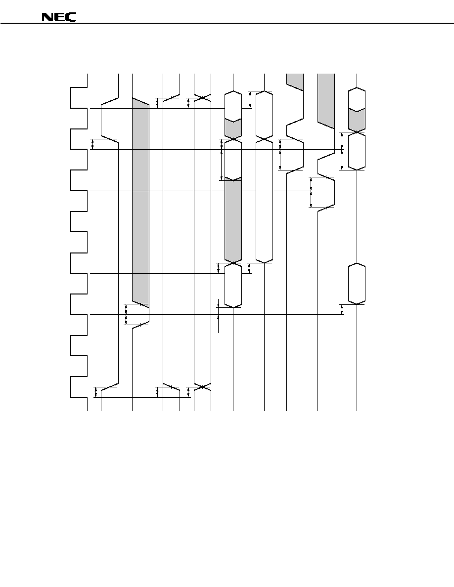
D
a
ta S
heet S
12689E
J2V
0
D
S
00
48
Á
Á
Á
Á
P
D
98405
CLK
ATTN_B
GNT_B
DR/W_B
SIZE2-SIZE0
AD31-AD0
BE3_B-BE0_B
RDY_B
(Normal mode)
RDY_B
(Early mode)
PAR3-PAR0
Address (output)
Data 1
(input)
BE 0 (output)
BE 1 (output)
(Output)
(Input)
t
DATTN
t
HGNT
t
SGNT
t
DATTN
t
DDRW
t
DSIZE
t
DSADD
t
FSADD
t
DSBE
t
DDRW
t
DSIZE
t
FSBE
t
HRDY
t
SRDY
t
HRDY
t
SRDY
t
HPAR2
t
DPAR2
t
HSDAT
Data 0
(input)
(Input)
t
SSDAT
t
SPAR2
DMA read access (Example: 2-word burst)
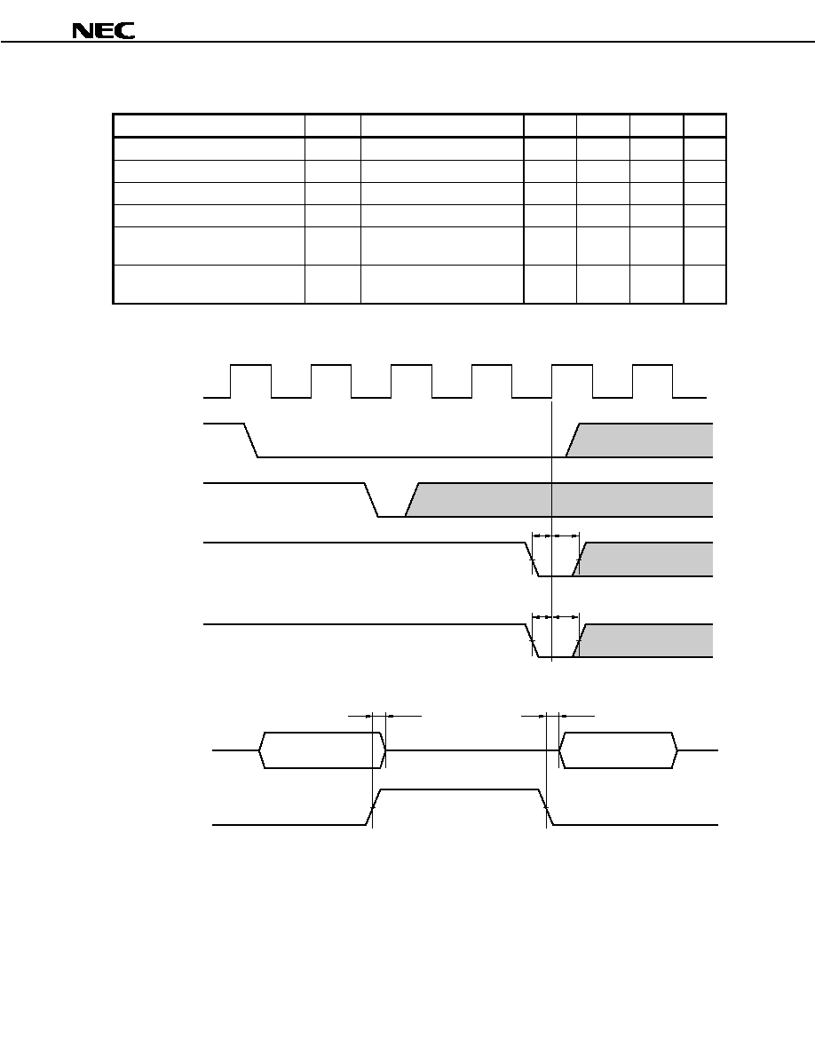
Data Sheet S12689EJ2V0DS00
49
Á
Á
Á
Á
PD98405
ABRT_B, ERR_B, and OE_B pins
Parameter
Symbol
Condition
MIN.
TYP.
MAX.
Unit
ABRT_B setup time
t
SABRT
8
ns
ABRT_B hold time
t
HABRT
3
ns
ERR_B setup time
t
SERR
8
ns
ERR_B hold time
t
HERR
3
ns
OE_B
AD/PAR output
determination time
t
DADOE
18
ns
OE_B
AD/PAR high-impedance
determination time
t
FADOE
18
ns
DMA abort/ERR_B timing
CLK
ATTN_B
GNT_B
ABRT_B
ERR_B
t
HABRT
t
SABRT
t
HERR
t
SERR
OE_B timing
AD31-AD0
PAR3-PAR0
Data 0
(output)
t
FADOE
OE_B
t
DADOE
Data 0
(output)
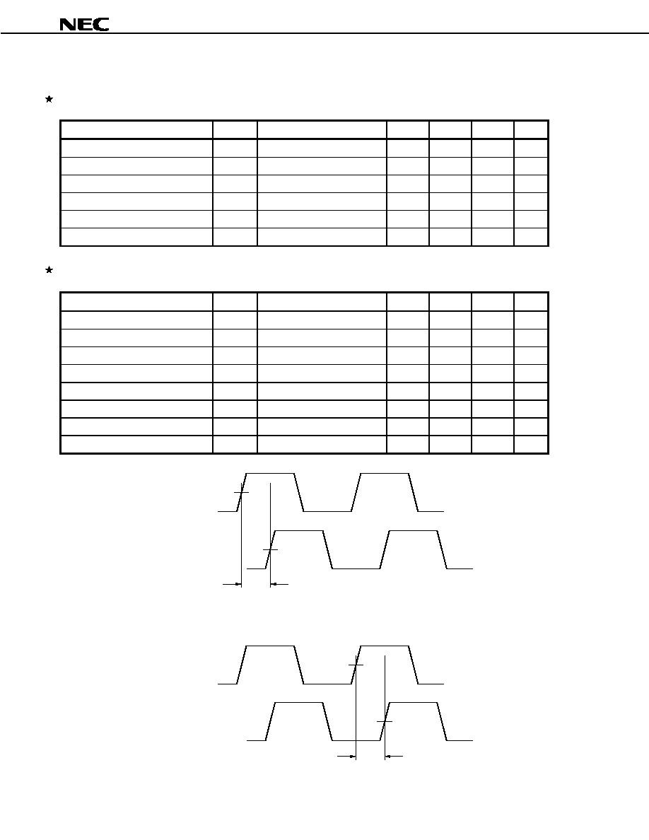
Data Sheet S12689EJ2V0DS00
50
Á
Á
Á
Á
PD98405
UTOPIA interface (external PHY mode)
Transmission operation
Parameter
Symbol
Condition
MIN.
TYP.
MAX.
Unit
SCLK
TCLK
delay time
t
DTCLK
15
ns
*
TCLK
Tx delay time
t
DTX
2
18
ns
*
TCLK
TSOC delay time
t
DTSOC
2
13.62
ns
*
TCLK
TENBL_B delay time
t
DTEN
2
13.66
ns
*
FULL_B setup time
t
SFULL
8
ns
FULL_B hold time
t
HFULL
1
ns
Reception operation
Parameter
Symbol
Condition
MIN.
TYP.
MAX.
Unit
SCLK
RCLK
delay time
t
DRCLK
15
ns
*
Rx setup time
t
SRX
8
ns
Rx hold time
t
HRX
1
ns
RSOC setup time
t
SRSOC
8
ns
RSOC hold time
t
HRSOC
1
ns
RCLK
RENBL_B delay time
t
DREN
2
13.63
ns
*
EMPTY_B setup time
t
SEMPT
8
ns
EMPTY_B hold time
t
HEMPT
1
ns
SCLK
TCLK
t
DTCLK
SCLK
RCLK
t
DRCLK
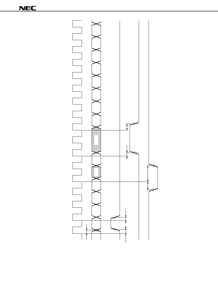
D
a
ta S
heet S
12689E
J2V
0
D
S
00
51
Á
Á
Á
Á
P
D
98405
TCLK
Tx7-Tx0
TSOC
TENBL_B
FULL_B
H1
H2
H3
H4
P1
P2
P3
P4
P5
P6
P7
P8
P9
`00H'
t
DTX
t
DTSOC
t
DTSOC
t
DTEN
t
DTEN
t
SFULL
t
HFULL
Invalid
H1-H4: ATM header
P1-P9: Payload data
UTOPIA interface (1)
Transmission timing
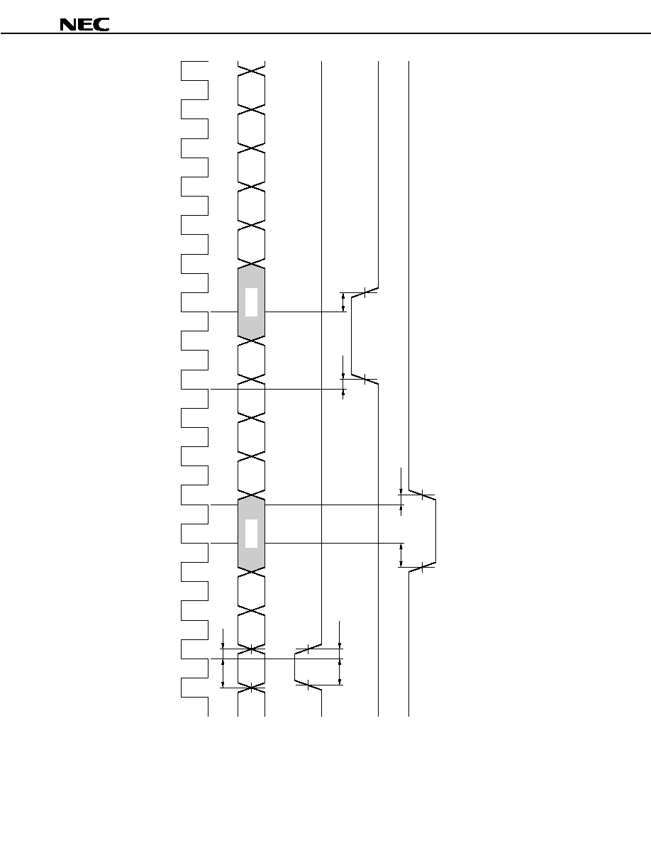
D
a
ta S
heet S
12689E
J2V
0
D
S
00
52
Á
Á
Á
Á
P
D
98405
Invalid
Invalid
RCLK
Rx7-Rx0
RSOC
RENBL_B
EMPTY_B
H1
H2
H3
H4
P2
P3
P4
P5
P6
P7
t
SRX
t
SRSOC
t
HRSOC
t
DREN
t
DREN
t
SEMPT
t
HEMPT
H1-H4: ATM header
P1-P7: Payload data
t
HRX
P1
H5
UTOPIA interface (2)
Reception timing
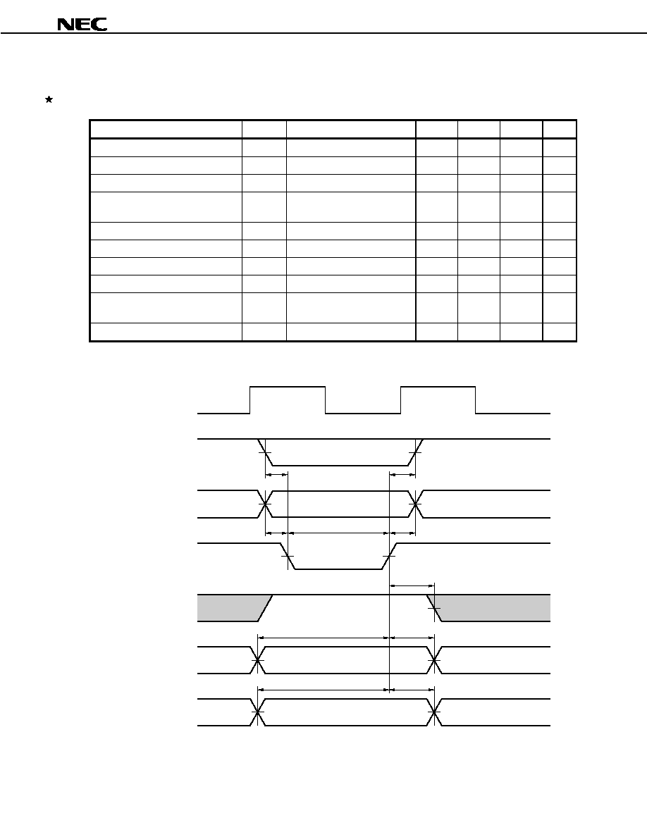
Data Sheet S12689EJ2V0DS00
53
Á
Á
Á
Á
PD98405
Control memory access
Write
Parameter
Symbol
Condition
MIN.
TYP.
MAX.
Unit
CA
CWE_B
setup time
t
SCWE
0
ns
CBE_B
CWE_B
setup time
t
SCWE2
0
ns
CWE_B low-level width
t
CWEL
1 t
SCLKL
¡ 2
ns
CWE_B
CD float time
t
FCD
0
1 t
SCLKL
+ 8.59
ns
*
CWE_B
COE_B delay time
t
DCOE
0
ns
CA hold time (vs CWE_B
)
t
HCA
0
ns
CBE_B hold time (vs CWE_B
)
t
HCBE
0
ns
CD output time (vs CWE_B
)
t
SCD
15
ns
*
CWE_B
CPAR float time
t
FCPAR
0
1 t
SCLKL
+ 8.65
ns
*
CPAR output time (vs CWE_B
)
t
SCPAR
15
ns
*
Write timing
SCLK
CBE3_B-
CBE0_B
CA18-CA0
CWE_B
COE_B
CD31-CD0
CPAR3-CPAR0
t
SCWE2
t
HCBE
t
SCWE
t
HCA
t
CWEL
t
SCD
t
FCD
t
SCPAR
t
FCPAR
t
DCOE
(Output)
(Output)
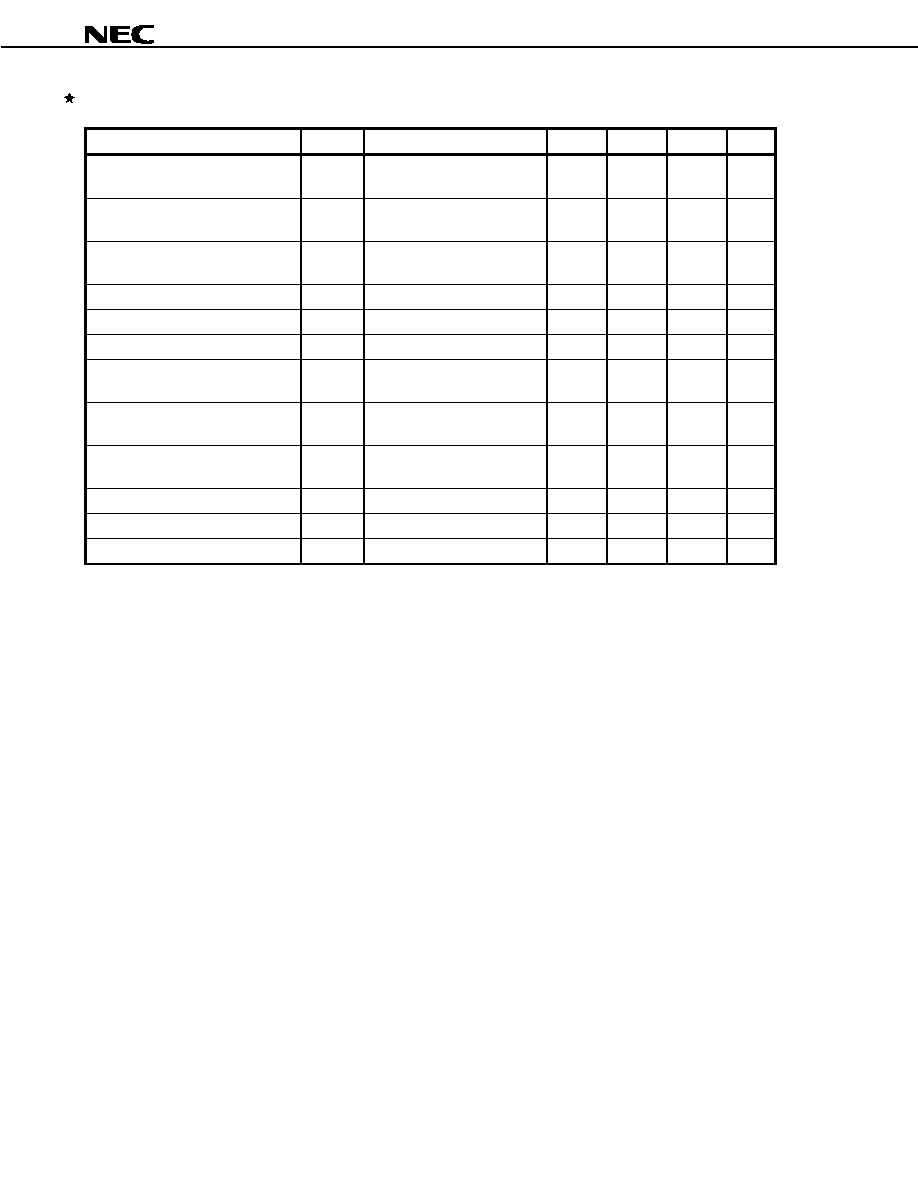
Data Sheet S12689EJ2V0DS00
54
Á
Á
Á
Á
PD98405
Read
Parameter
Symbol
Condition
MIN.
TYP.
MAX.
Unit
Permissible CD delay time
(vs CBE_B
)
t
DCDCB
1 t
CYSCLK
¡ 18
ns
*
Permissible CD delay time (vs CA)
t
DCDCA
1 t
CYSCLK
¡ 18
ns
*
Permissible CD delay time
(vs COE_B
)
t
DCDCO
1 t
CYSCLK
¡ 18
ns
*
CD hold time (vs CBE_B
)
t
HCDCB
0
ns
CD hold time (vs CA)
t
HCDCA
0
ns
CD hold time (vs COE_B
)
t
HCDCO
0
ns
Permissible CPAR hold time
(vs CBE_B
)
t
DCPCB
1 t
CYSCLK
¡ 18
ns
*
Permissible CPAR hold time (vs CA)
t
DCPCA
1 t
CYSCLK
¡ 18
ns
*
Permissible CPAR hold time
(vs COE_B
)
t
DCPCO
1 t
CYSCLK
¡ 18
ns
*
CPAR hold time (vs CBE_B
)
t
HCPCB
0
ns
CPAR hold time (vs CA)
t
HCPCA
0
ns
CPAR hold time (vs COE_B
)
t
HCPCO
0
ns
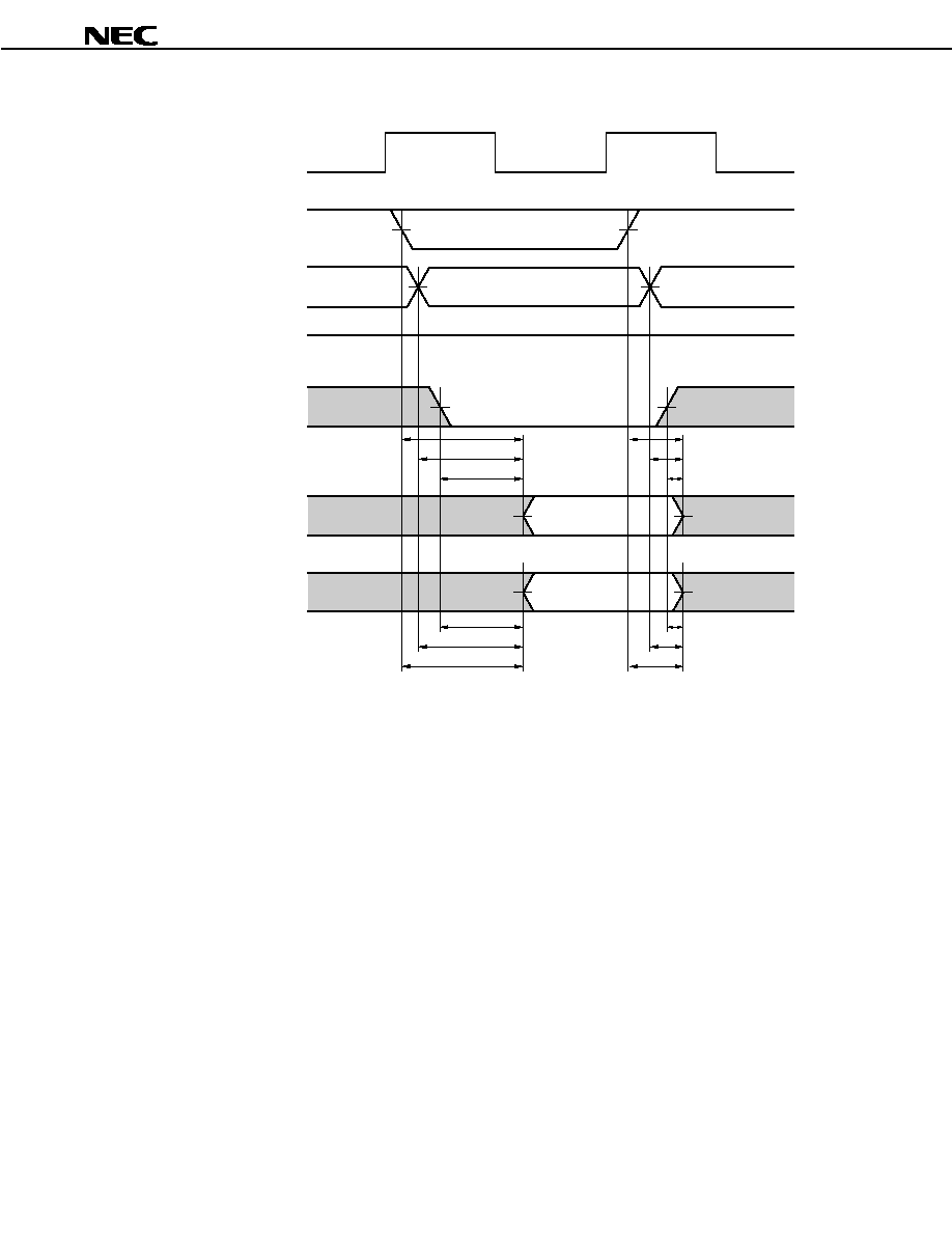
Data Sheet S12689EJ2V0DS00
55
Á
Á
Á
Á
PD98405
Read timing
SCLK
CBE3_B-
CBE0_B
CA18-CA0
COE_B
CWE_B
CD31-CD0
(Input)
CPAR3-CPAR0
(Input)
t
HCDCB
t
HCDCA
t
HCDCO
t
DCDCB
t
DCDCA
t
DCDCO
t
HCPCO
t
HCPCA
t
HCPCB
t
DCPCO
t
DCPCA
t
DCPCB
"H"
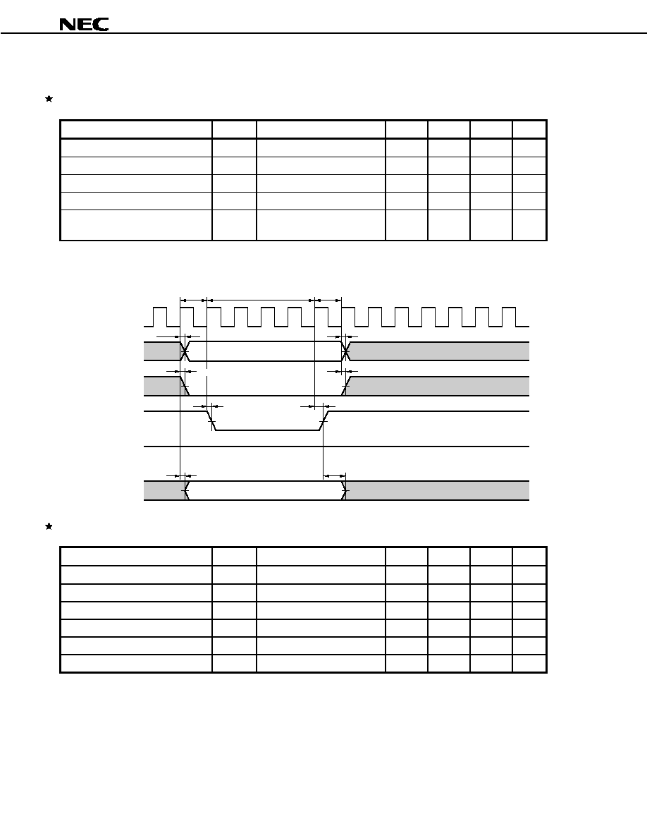
Data Sheet S12689EJ2V0DS00
56
Á
Á
Á
Á
PD98405
PHY status access
Write
Parameter
Symbol
Condition
MIN.
TYP.
MAX.
Unit
SCLK
CA delay time
t
DPCA
20
ns
SCLK
PHRW_B delay time
t
DPHRW
20
ns
SCLK
PHCE_B delay time
t
DPHCE
20
ns
SCLK
CD delay time
t
DPCD
23
ns
*
PHCE_B
CD float time
t
FPCD
1 t
CYSCLK
¡ 10
1 t
CYSCLK
+ 10
ns
Write timing
SCLK
CA18-CA0
PHRW_B
PHCE_B
PHOE_B
CD31-CD0
t
DPCA
t
DPCA
t
DPHRW
t
DPHRW
t
DPHCE
t
DPHCE
t
DPCD
t
FPCD
1 clock
4 clocks
1 clock
(Output)
"H"
Read
Parameter
Symbol
Condition
MIN.
TYP.
MAX.
Unit
CD setup time
t
SPCD
10
ns
*
CD hold time
t
HPOECD
0
ns
SCLK
CA delay time
t
DPCA
20
ns
SCLK
PHRW_B delay time
t
DPHRW
20
ns
SCLK
PHCE_B delay time
t
DPHCE
20
ns
SCLK
PHOE_B delay time
t
DPHOE
20
ns
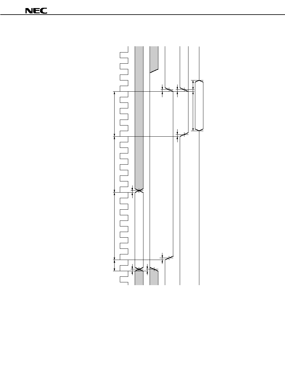
D
a
ta S
heet S
12689E
J2V
0
D
S
00
57
Á
Á
Á
Á
P
D
98405
SCLK
CA18-CA0
PHRW_B
PHCE_B
PHOE_B
CD31-CD0
t
DPCA
t
DPHRW
t
DPHCE
t
DPCA
t
DPHOE
t
DPHOE
t
DPHCE
t
SPCD
t
HPOECD
1 clock
6 clocks
5 clocks
4 clocks
(Input)
Read timing
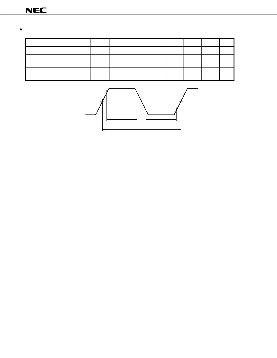
Data Sheet S12689EJ2V0DS00
58
Á
Á
Á
Á
PD98405
PMD serial interface (internal PHY mode)
Parameter
Symbol
Condition
MIN.
TYP.
MAX.
Unit
REFCLK cycle time
t
CYRF
¡20 ppm
51.4403
+20 ppm
ns
*
REFCLK high-level width
t
WRFH
0.4
Î
t
CYRF
0.4
Î
t
CYRF
ns
*
REFCLK low-level width
t
WRFL
0.4
Î
t
CYRF
0.4
Î
t
CYRF
ns
*
t
WRFH
t
WRFL
t
CYRF
REFCLK
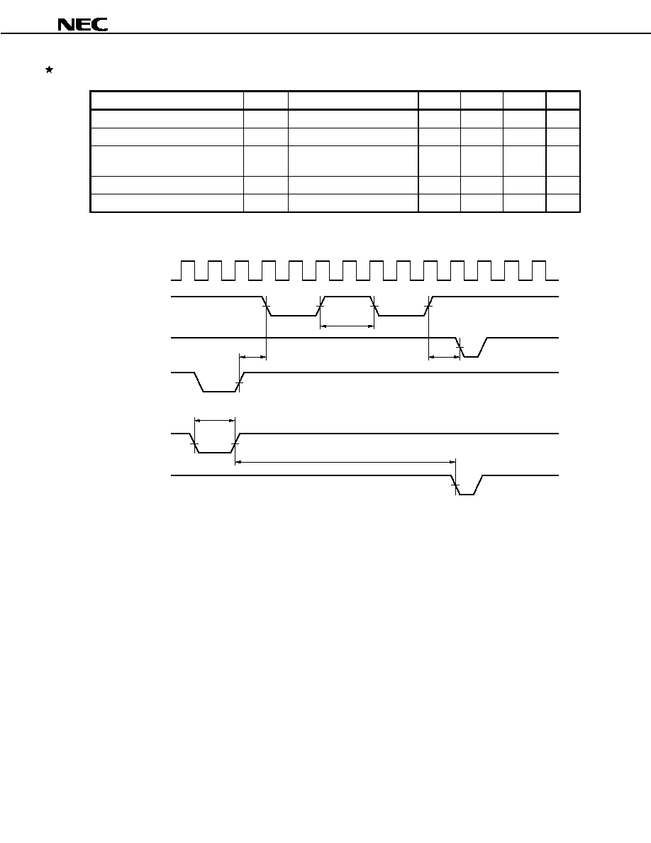
Data Sheet S12689EJ2V0DS00
59
Á
Á
Á
Á
PD98405
Others
Parameter
Symbol
Condition
MIN.
TYP.
MAX.
Unit
SEL_B recovery time
t
RVSEL
2
t
CYCLK
SEL_B
GNT_B
recovery time
t
RVSM
1
t
CYCLK
RDY_B
SEL_B
recovery time
t
RVMS
RDY_B mode during normal
operation
1
t
CYCLK
RST_B input pulse width
t
RSTL
1
t
CYCLK
RST_B
SEL_B
recovery time
t
RSTSL
20
t
CYCLK
Others timing
CLK
SEL_B
GNT_B
RDY_B
RST_B
SEL_B
t
RVSEL
t
RVSM
t
RVMS
t
RSTL
t
RSTSL
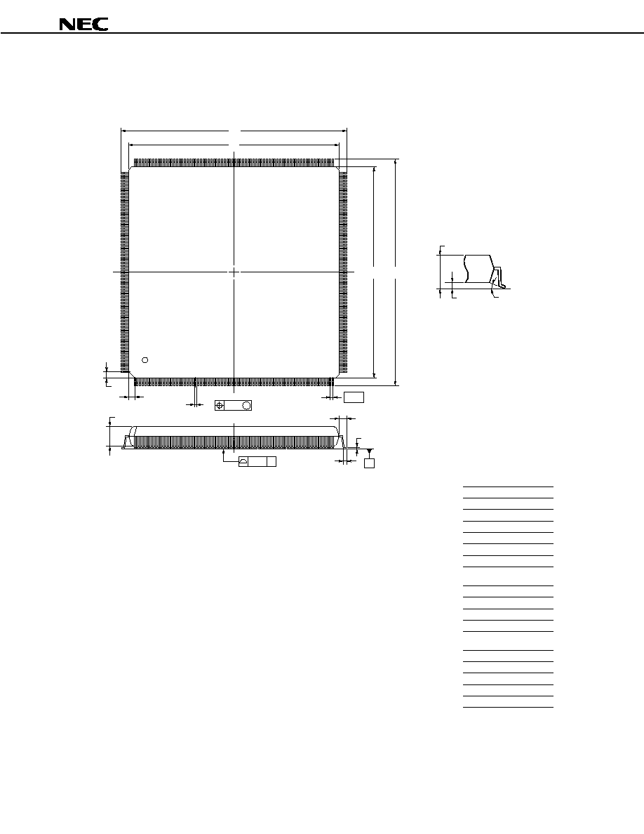
Data Sheet S12689EJ2V0DS00
60
Á
Á
Á
Á
PD98405
3. PACKAGE DRAWING
228
229
153
152
77
76
304
1
S
304 PIN PLASTIC QFP (FINE PITCH) (40x40)
NOTE
Each lead centerline is located within 0.10 mm of
its true position (T.P.) at maximum material condition.
ITEM
MILLIMETERS
F
G
1.25
1.25
A
42.6
▒
0.2
B
C
40.0
▒
0.2
40.0
▒
0.2
D
42.6
▒
0.2
H
0.22
I
0.10
S
4.3 MAX.
K
1.3
▒
0.2
L
0.5
▒
0.2
M
0.145
N
0.10
+
0.05
-
0.04
J
0.5 (T.P.)
P304GL-50-NMU, PMU-3
+
0.055
-
0.045
R
5
░▒
5
░
detail of lead end
Q
0.4
▒
0.1
P
3.7
▒
0.1
Q
R
K
M
L
P
H
G
F
M
A
B
C
D
S
J
N
I
S
Data Sheet S12689EJ2V0DS00
61
Á
Á
Á
Á
PD98405
4. RECOMMENDED SOLDERING CONDITIONS
Solder this product under the following recommended conditions.
For details of the recommended soldering conditions, refer to information document Semiconductor Device
Mounting Technology Manual (C10535E).
For soldering methods and conditions other than those recommended, consult NEC.
Surface-mount type
À
Á
Á
Á
Á
PD98405GL-PMU: 304-pin plastic QFP (0.5-mm fine pitch) (40
Î
Î
Î
Î
40 mm)
Soldering Method(s)
Soldering Conditions
Recommended
Conditions Symbol
Infrared reflow
Package peak temperature: 235░C, Time: 30 sec max. (210░C min.),
Number of times: once, Number of days: 3
Note
(after that, prebaking is
necessary at 125░C for 20 hours)
IR35-203-1
Partial pin heating
Pin temperature: 300░C max., Time: 3 sec. Max. (per device side)
¡
Note Number of days in storage after the dry pack has been opened. The storage conditions are at 25░C, 65%
RH MAX.

Data Sheet S12689EJ2V0DS00
62
Á
Á
Á
Á
PD98405
[MEMO]

Data Sheet S12689EJ2V0DS00
63
Á
Á
Á
Á
PD98405
[MEMO]

Á
Á
Á
Á
PD98405
À
The information in this document is subject to change without notice. Before using this document, please
confirm that this is the latest version.
À
No part of this document may be copied or reproduced in any form or by any means without the prior written
consent of NEC Corporation. NEC Corporation assumes no responsibility for any errors which may appear in
this document.
À
NEC Corporation does not assume any liability for infringement of patents, copyrights or other intellectual property
rights of third parties by or arising from use of a device described herein or any other liability arising from use
of such device. No license, either express, implied or otherwise, is granted under any patents, copyrights or other
intellectual property rights of NEC Corporation or others.
À
Descriptions of circuits, software, and other related information in this document are provided for illustrative
purposes in semiconductor product operation and application examples. The incorporation of these circuits,
software, and information in the design of the customer's equipment shall be done under the full responsibility
of the customer. NEC Corporation assumes no responsibility for any losses incurred by the customer or third
parties arising from the use of these circuits, software, and information.
À
While NEC Corporation has been making continuous effort to enhance the reliability of its semiconductor devices,
the possibility of defects cannot be eliminated entirely. To minimize risks of damage or injury to persons or
property arising from a defect in an NEC semiconductor device, customers must incorporate sufficient safety
measures in its design, such as redundancy, fire-containment, and anti-failure features.
À
NEC devices are classified into the following three quality grades:
"Standard", "Special", and "Specific". The Specific quality grade applies only to devices developed based on a
customer designated "quality assurance program" for a specific application. The recommended applications of
a device depend on its quality grade, as indicated below. Customers must check the quality grade of each device
before using it in a particular application.
Standard: Computers, office equipment, communications equipment, test and measurement equipment,
audio and visual equipment, home electronic appliances, machine tools, personal electronic
equipment and industrial robots
Special: Transportation equipment (automobiles, trains, ships, etc.), traffic control systems, anti-disaster
systems, anti-crime systems, safety equipment and medical equipment (not specifically designed
for life support)
Specific: Aircraft, aerospace equipment, submersible repeaters, nuclear reactor control systems, life
support systems or medical equipment for life support, etc.
The quality grade of NEC devices is "Standard" unless otherwise specified in NEC's Data Sheets or Data Books.
If customers intend to use NEC devices for applications other than those specified for Standard quality grade,
they should contact an NEC sales representative in advance.
M7 98. 8