©
1993
DATA SHEET
The
µ
PD4721 is a high-breakdown voltage silicon gate CMOS line driver/receiver based on the EIA/TIA-232-
E standard. The internal DC/DC converter can switch between multiple voltages, realizing the allowing it to
operate with a single +3.3 V or +5 V power supply. It also provides standby function.
This IC incorporates 2 driver circuits and 2 receiver circuits. An RS-232 interface circuit can be easily
configured by connecting 5 capacitors externally.
FEATURES
· Conforms to EIA/TIA-232-E (former name, RS-232C) standards
· Selectable +3.3 V/+5 V single power supply (selected by V
CHA
pin)
· By setting the standby pin to a low level (standby mode), circuit current can be reduced. At such times,
the driver output is in a high-impedance state.
ORDERING INFORMATION
Part number
Package
µ
PD4721GS-GJG
20-pin plastic SSOP (300 mil)
MOS INTEGRATED CIRCUIT
µ
P D 4 7 2 1
Document No.
S12198EJ2V0DS00 (2nd edition)
(Previous No. IC-3279)
Date Published January 1997 N
Printed in Japan
RS-232 LINE DRIVER/RECEIVER AT 3.3 V/5 V

2
µ
PD4721
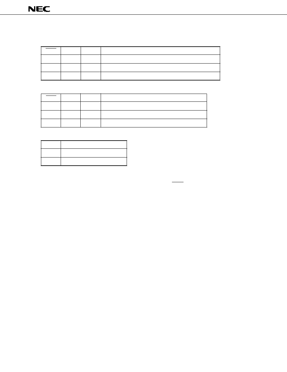
BLOCK DIAGRAM/PIN CONFIGURATION (Top View)
Note 1. V
DD
and V
SS
are output pins stepped up internally. These pins should not be loaded directly.
2. Capacitors C
1
to C
5
with a breakdown voltage of 20 V or higher are recommended. And it is
recommended to insert the capacitor that is 0.1
µ
F to 1
µ
F between V
CC
and GND.
3. If V
CHA
is kept low level (in 5 V mode), capacitor C
5
is not necessary.
4. The pull-up resistors at driver input are active resistors.
1
2
3
4
5
6
7
8
9
10
20
19
18
17
16
15
14
13
12
11
D
IN1
D
IN2
R
OUT1
R
OUT2
STBY
V
CHA
D
OUT1
D
OUT2
R
IN1
R
IN2
V
DD
C
1
+
V
CC
C
1
C
5
+
C
5
C
4
+
GND
C
4
V
SS
+10 V
C
3
C
1
C
5
10 V
+
C
2
C
4
+
+
+
Note 4
300
300
5.5 k
5.5 k
+3.3 V
or
+5 V
+
3
µ
PD4721
Truth Table
Driver
STBY
D
IN
D
OUT
Remarks
L
×
Z
Standby mode (DC/DC converter is stopped)
H
L
H
Space level output
H
H
L
Mark level output
Receiver
STBY
R
IN
R
OUT
Remarks
L
×
H
Standby mode (DC/DC converter is stopped)
H
L
H
Mark level input
H
H
L
Space level input
3 V
5 V switching
Note 5
V
CHA
Operating mode
L
5 V mode (double step-up)
H
3 V mode (3 times step-up)
H: high-level, L: low-level, Z: high-impedance,
×
: H or L
Note 5. When switching V
CHA
, standby mode must be selected (STBY = L).
4
µ
PD4721
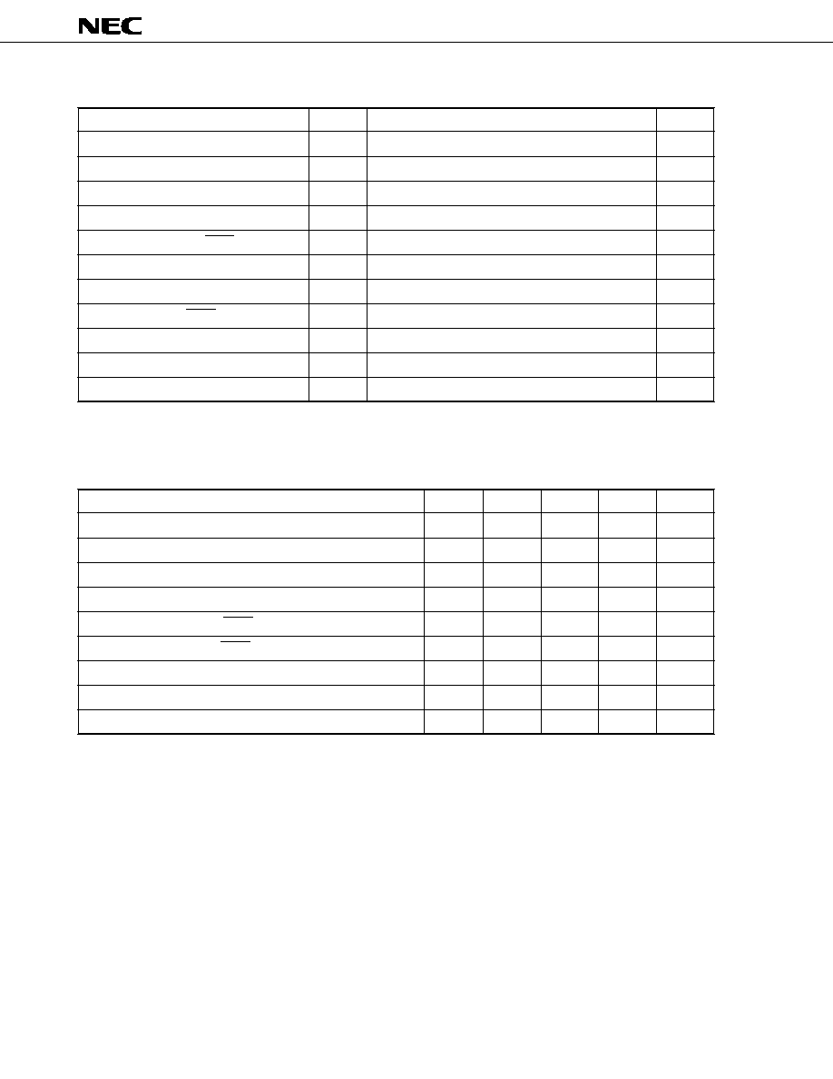
ABSOLUTE MAXIMUM RATINGS (T
A
= 25
°
C)
Parameter
Symbol
Ratings
Unit
Supply Voltage (V
CHA
= L)
V
CC
0.5 to +7.0
V
Supply Voltage (V
CHA
= H)
V
CC
0.5 to +4.5
V
Driver Input Voltage
D
IN
0.5 to V
CC
+0.5
V
Receiver Input Voltage
R
IN
30.0 to +30.0
V
Control Input Voltage (STBY, V
CHA
)
V
IN
0.5 to V
CC
+0.5
V
Driver Output Voltage
D
OUT
25.0 to +25.0
Note 6
V
Receiver Output Voltage
R
OUT
0.5 to V
CC
+0.5
V
Input Current (D
IN
, STBY, V
CHA
)
I
IN
±
20.0
mA
Operating Ambient Temperature
T
A
40 to +85
°
C
Storage Temperature
T
stg
55 to +150
°
C
Total Power Dissipation
P
T
0.5
W
Note 6. Pulse width = 1 ms, duty = 10 % MAX.
RECOMMENDED OPERATING CONDITIONS
Parameter
Symbol
MIN.
TYP.
MAX.
Unit
Supply Voltage (V
CHA
= L, 5 V mode)
V
CC
4.5
5.0
5.5
V
Supply Voltage (V
CHA
= H, 3 V mode)
V
CC
3.0
3.3
3.6
V
High-Level Input Voltage (D
IN
)
V
IH
2.0
V
CC
V
Low-Level Input Voltage (D
IN
)
V
IL
0
0.8
V
High-Level Input Voltage (STBY, V
CHA
)
V
IH
2.4
V
CC
V
Low-Level Input Voltage (STBY, V
CHA
)
V
IL
0
0.6
V
Receiver Input Voltage
R
IN
30
+30
V
Operating Ambient Temperature
T
A
40
+85
°
C
Capacitance of External Capacitor
Note 7
0.33
4.7
µ
F
Note 7. In low temperature (below 0 °C), the capacitance of electrolytic capacitor becomes lower. Therefore,
set higher values when using in low temperature.
Concerning the wiring length between the capacitor and the IC, the shorter the better.
Capacitors with good frequency characteristics such as tantalum capacitors, laminated ceramic
capacitors, and aluminum electrolytic capacitors for switching power supply are recommended for the
external capacitors.

5
µ
PD4721
ELECTRICAL SPECIFICATIONS (TOTAL)
(Unless otherwise specified, T
A
= 40 to +85
°
C, C
1
to C
5
= 1
µ
F)
Parameter
Symbol
Conditions
MIN.
TYP.
MAX.
Unit
V
CC
= +3.3 V, No load, R
IN
pin OPEN,
STBY = H
V
CC
= +5.0 V, No load, R
IN
pin OPEN,
STBY = H
V
CC
= +3.3 V, R
L
= 3 k
(D
OUT
), D
IN
= GND,
R
IN
, R
OUT
pin OPEN, STBY = H
V
CC
= +5.0 V,R
L
= 3 k
(D
OUT
), D
IN
= GND,
R
IN
, R
OUT
pin OPEN, STBY = H
V
CC
= +3.3 V, No load, D
IN
and R
IN
pins are OPEN, STBY = L, T
A
= 25
°
C
V
CC
= +3.3 V, No load, D
IN
and R
IN
pins are OPEN, STBY = L
V
CC
= +5.0 V, No load, D
IN
and R
IN
pins are OPEN, STBY = L, T
A
= 25
°
C
V
CC
= +5.0 V, No load, D
IN
and R
IN
pins are OPEN, STBY = L
High-Level Input Voltage
V
IH
V
CC
= +3.0 to +5.5 V, STBY, V
CHA
pin
2.4
V
Low-Level Input Voltage
V
IL
V
CC
= +3.0 to +5.5 V, STBY, V
CHA
pin
0.6
V
High-Level Input Current
I
IH
V
CC
= +5.5 V, V
I
= +5.5 V, STBY, V
CHA
pin
1
µ
A
Low-Level Input Current
I
IL
V
CC
= +5.5 V, V
I
= 0 V, STBY, V
CHA
pin
1
µ
A
Driver input and receiver input
V
CC
= +3.3 V, for GND, f = 1 MHz
Driver input and receiver input
V
CC
= +5.0 V, for GND, f = 1 MHz
STBY -- V
CHA
Time
t
SCH
V
CC
= +3.0 to +5.5 V, STBY
V
CHA
,
Note 8
1
µ
s
V
CHA
-- STBY Time
t
CHS
V
CC
= +3.0 to +5.5 V, V
CHA
STBY
,
Note 8
1
µ
s
STBY -- V
CC
Time
t
SC
V
CC
= +3.0 to +5.5 V, STBY
V
CC
,
Note 8
1
µ
s
V
CC
-- STBY Time
t
CS
V
CC
= +3.0 to +5.5 V, V
CC
STBY
,
Note 8
1
µ
s
* The TYP. values are for reference at T
A
= 25
°
C.
Note 8. Measuring point
Circuit Current
I
CC1
4.5
9
mA
6.5
13
mA
Circuit Current
I
CC2
19
24
mA
14
18
mA
1
3
µ
A
2
5
µ
A
10
µ
A
5
µ
A
Circuit Current at Standby
I
CC3
10
pF
10
pF
Input Capacitance
C
IN
3.3 V
0.6 V
2.4 V
0.6 V
0.6 V
0.6 V
2.4 V
0.6 V
4.5 V
3.6 V
4.5 V
3.6 V
t
SCH
t
CHS
t
SCH
t
CHS
t
SC
t
CS
t
SC
t
CS
5 V
0.6 V
0 V
3.3 V
5 V
0 V
STBY
V
CHA
V
CC
3.3 V