Document Outline
- COVER
- Features
- Ordering Information
- Pin Configurations
- Block Diagram
- Electrical Specifications
- JTAG Specification
- Package Drawing

The mark shows major revised points.
The information in this document is subject to change without notice. Before using this document, please
confirm that this is the latest version.
Not all products and/or types are available in every country. Please check with an NEC Electronics
sales representative for availability and additional information.
MOS INTEGRATED CIRCUIT
µ
PD44325082, 44325092, 44325182, 44325362
36M-BIT QDR
TM
II SRAM
2-WORD BURST OPERATION
Document No. M16783EJ1V0DS00 (1st edition)
Date Published October 2004 NS CP(K)
Printed in Japan
PRELIMINARY DATA SHEET
2003
Description
The
µ
PD44325082 is a 4,194,304-word by 8-bit, the
µ
PD44325092 is a 4,194,304-word by 9-bit, the
µ
PD44325182 is a
2,097,152-word by 18-bit and the
µ
PD44325362 is a 1,048,576-word by 36-bit synchronous quad data rate static RAM
fabricated with advanced CMOS technology using full CMOS six-transistor memory cell.
The
µ
PD44325082,
µ
PD44325092,
µ
PD44325182 and
µ
PD44325362 integrate unique synchronous peripheral
circuitry and a burst counter. All input registers controlled by an input clock pair (K and /K) are latched on the positive
edge of K and /K.
These products are suitable for application which require synchronous operation, high speed, low voltage, high density
and wide bit configuration.
These products are packaged in 165-pin PLASTIC FBGA.
Features
· 1.8 ± 0.1 V power supply and HSTL I/O
· DLL circuitry for wide output data valid window and future frequency scaling
· Separate independent read and write data ports with concurrent transactions
· 100% bus utilization DDR READ and WRITE operation
· Two-tick burst for low DDR transaction size
· Two input clocks (K and /K) for precise DDR timing at clock rising edges only
· Two output clocks (C and /C) for precise flight time and clock skew matching-clock
and data delivered together to receiving device
· Internally self-timed write control
· Clock-stop capability with
µ
s restart
· User programmable impedance output
· Fast clock cycle time : 4.0 ns (250 MHz), 5.0 ns (200 MHz)
· Simple control logic for easy depth expansion
· JTAG boundary scan
2
Preliminary Data Sheet
M16783EJ1V0DS
µ
PD44325082, 44325092, 44325182, 44325362
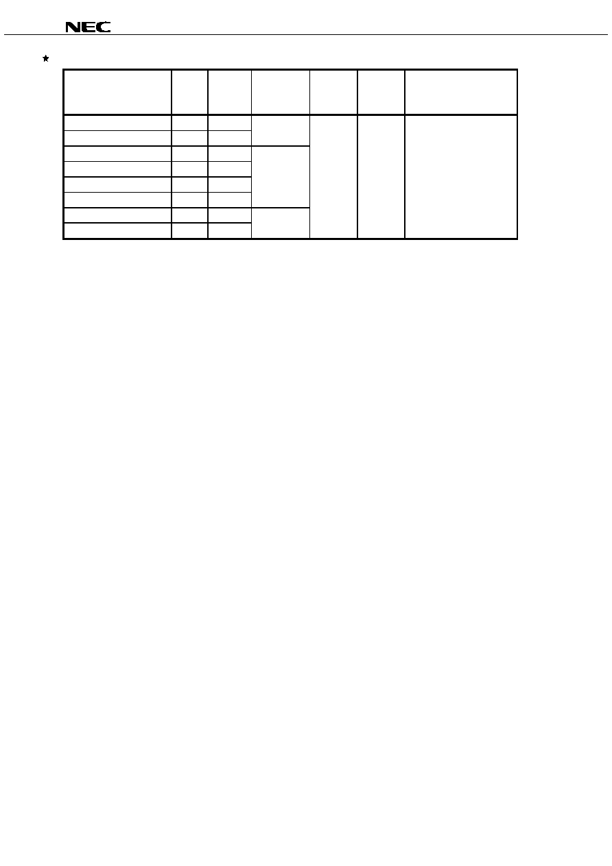
Ordering Information
Part number
Cycle
Clock
Organization Core Supply
I/O
Package
Time Frequency (word
x
bit) Voltage Interface
ns MHz
V
µ
PD44325082F5-E40-EQ2
4.0
250
4 M x 8-bit
1.8 ± 0.1
HSTL
165-pin PLASTIC
µ
PD44325082F5-E50-EQ2
5.0
200
FBGA (13 x 15)
µ
PD44325092F5-E40-EQ2
4.0
250
4 M x 9-bit
µ
PD44325092F5-E50-EQ2 5.0
200
µ
PD44325182F5-E40-EQ2
4.0
250
2 M x 18-bit
µ
PD44325182F5-E50-EQ2 5.0
200
µ
PD44325362F5-E40-EQ2
4.0
250
1M x 36-bit
µ
PD44325362F5-E50-EQ2 5.0
200
3
Preliminary Data Sheet
M16783EJ1V0DS
µ
PD44325082, 44325092, 44325182, 44325362
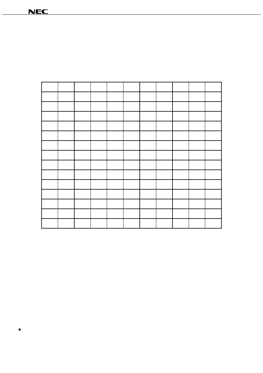
Pin Configurations
/
××× indicates active low signal.
165-pin PLASTIC FBGA (13 x 15)
(Top View)
[
µ
PD44325082F5-EQ2]
1 2 3 4 5 6 7 8 9 10
11
A /CQ V
SS
A /W
/NW1
/K NC /R A A CQ
B
NC NC NC A NC K /NW0 A NC NC Q3
C NC NC NC V
SS
A A A V
SS
NC NC D3
D
NC D4 NC V
SS
V
SS
V
SS
V
SS
V
SS
NC NC NC
E NC NC Q4 V
DD
Q V
SS
V
SS
V
SS
V
DD
Q NC D2 Q2
F NC NC NC V
DD
Q V
DD
V
SS
V
DD
V
DD
Q NC NC NC
G NC D5 Q5 V
DD
Q V
DD
V
SS
V
DD
V
DD
Q NC NC NC
H /DLL V
REF
V
DD
Q V
DD
Q V
DD
V
SS
V
DD
V
DD
Q V
DD
Q V
REF
ZQ
J NC NC NC V
DD
Q V
DD
V
SS
V
DD
V
DD
Q NC Q1 D1
K NC NC NC V
DD
Q V
DD
V
SS
V
DD
V
DD
Q NC NC NC
L NC Q6 D6 V
DD
Q V
SS
V
SS
V
SS
V
DD
Q NC NC Q0
M NC NC NC V
SS
V
SS
V
SS
V
SS
V
SS
NC NC D0
N
NC D7 NC V
SS
A A A V
SS
NC NC NC
P
NC
NC
Q7 A A C A A NC
NC
NC
R
TDO
TCK A A A /C A A A
TMS
TDI
A
: Address inputs
TMS
: IEEE 1149.1 Test input
D0 to D7
: Data inputs
TDI
: IEEE 1149.1 Test input
Q0 to Q7
: Data outputs
TCK
: IEEE 1149.1 Clock input
/R
: Read input
TDO
: IEEE 1149.1 Test output
/W
: Write input
V
REF
: HSTL input reference input
/NW0, /NW1
: Nibble Write data select
V
DD
: Power Supply
K, /K
: Input clock
V
DD
Q
: Power Supply
C, /C
: Output clock
V
SS
:
Ground
CQ, /CQ
: Echo clock
NC
: No connection
ZQ
: Output impedance matching
/DLL
: DLL disable
Remarks 1. Refer to Package Drawing for the index mark.
2. 2A and 7A are expansion addresses: 2A for 72Mb and 7A for 144Mb.

4
Preliminary Data Sheet
M16783EJ1V0DS
µ
PD44325082, 44325092, 44325182, 44325362
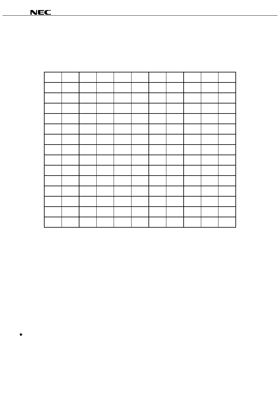
165-pin PLASTIC FBGA (13 x 15)
(Top View)
[
µ
PD44325092F5-EQ2]
1 2 3 4 5 6 7 8 9 10
11
A /CQ V
SS
A /W NC /K NC /R A A CQ
B
NC NC NC A NC K /BW0 A NC NC Q4
C NC NC NC V
SS
A A A V
SS
NC NC D4
D
NC D5 NC V
SS
V
SS
V
SS
V
SS
V
SS
NC NC NC
E NC NC Q5 V
DD
Q V
SS
V
SS
V
SS
V
DD
Q NC D3 Q3
F NC NC NC V
DD
Q V
DD
V
SS
V
DD
V
DD
Q NC NC NC
G NC D6 Q6 V
DD
Q V
DD
V
SS
V
DD
V
DD
Q NC NC NC
H /DLL V
REF
V
DD
Q V
DD
Q V
DD
V
SS
V
DD
V
DD
Q V
DD
Q V
REF
ZQ
J NC NC NC V
DD
Q V
DD
V
SS
V
DD
V
DD
Q NC Q2 D2
K NC NC NC V
DD
Q V
DD
V
SS
V
DD
V
DD
Q NC NC NC
L NC Q7 D7 V
DD
Q V
SS
V
SS
V
SS
V
DD
Q NC NC Q1
M NC NC NC V
SS
V
SS
V
SS
V
SS
V
SS
NC NC D1
N
NC D8 NC V
SS
A A A V
SS
NC NC NC
P
NC
NC
Q8 A A C A A NC
D0
Q0
R
TDO
TCK A A A /C A A A
TMS
TDI
A
: Address inputs
TMS
: IEEE 1149.1 Test input
D0 to D8
: Data inputs
TDI
: IEEE 1149.1 Test input
Q0 to Q8
: Data outputs
TCK
: IEEE 1149.1 Clock input
/R
: Read input
TDO
: IEEE 1149.1 Test output
/W
: Write input
V
REF
: HSTL input reference input
/BW0
: Byte Write data select
V
DD
: Power Supply
K, /K
: Input clock
V
DD
Q
: Power Supply
C, /C
: Output clock
V
SS
:
Ground
CQ, /CQ
: Echo clock
NC
: No connection
ZQ
: Output impedance matching
/DLL
: DLL disable
Remarks 1. Refer to Package Drawing for the index mark.
2. 2A and 7A are expansion addresses: 2A for 72Mb and 7A for 144Mb.
5
Preliminary Data Sheet
M16783EJ1V0DS
µ
PD44325082, 44325092, 44325182, 44325362
165-pin PLASTIC FBGA (13 x 15)
(Top View)
[
µ
PD44325182F5-EQ2]
1 2 3 4 5 6 7 8 9 10
11
A /CQ V
SS
A /W
/BW1
/K NC /R A V
SS
CQ
B
NC Q9 D9 A NC K /BW0 A NC NC Q8
C NC NC D10 V
SS
A A A V
SS
NC Q7 D8
D NC D11 Q10 V
SS
V
SS
V
SS
V
SS
V
SS
NC NC D7
E NC NC Q11 V
DD
Q V
SS
V
SS
V
SS
V
DD
Q NC D6 Q6
F NC Q12 D12 V
DD
Q V
DD
V
SS
V
DD
V
DD
Q NC NC Q5
G NC D13 Q13 V
DD
Q V
DD
V
SS
V
DD
V
DD
Q NC NC D5
H /DLL V
REF
V
DD
Q V
DD
Q V
DD
V
SS
V
DD
V
DD
Q V
DD
Q V
REF
ZQ
J NC NC D14 V
DD
Q V
DD
V
SS
V
DD
V
DD
Q NC Q4 D4
K NC NC Q14 V
DD
Q V
DD
V
SS
V
DD
V
DD
Q NC D3 Q3
L NC Q15 D15 V
DD
Q V
SS
V
SS
V
SS
V
DD
Q NC NC Q2
M NC NC D16 V
SS
V
SS
V
SS
V
SS
V
SS
NC Q1 D2
N NC D17 Q16 V
SS
A A A V
SS
NC NC D1
P
NC
NC
Q17
A A C A A NC
D0
Q0
R
TDO
TCK A A A /C A A A
TMS
TDI
A
: Address inputs
TMS
: IEEE 1149.1 Test input
D0 to D17
: Data inputs
TDI
: IEEE 1149.1 Test input
Q0 to Q17
: Data outputs
TCK
: IEEE 1149.1 Clock input
/R
: Read input
TDO
: IEEE 1149.1 Test output
/W
: Write input
V
REF
: HSTL input reference input
/BW0, /BW1
: Byte Write data select
V
DD
: Power Supply
K, /K
: Input clock
V
DD
Q
: Power Supply
C, /C
: Output clock
V
SS
:
Ground
CQ, /CQ
: Echo clock
NC
: No connection
ZQ
: Output impedance matching
/DLL
: DLL disable
Remarks 1. Refer to Package Drawing for the index mark.
2. 2A and 10A are expansion addresses: 10A for 72Mb and 2A for 144Mb.