
The information in this document is subject to change without notice. Before using this document, please
confirm that this is the latest version.
Not all devices/types available in every country. Please check with local NEC representative for
availability and additional information.
®
2001
MOS INTEGRATED CIRCUIT
Á
Á
Á
Á
PD4382323, 4382363
8M-BIT CMOS SYNCHRONOUS FAST SRAM
PIPELINED OPERATION
DOUBLE CYCLE DESELECT
Document No. M15393EJ1V0DS00 (1st edition)
Date Published February 2001 NS CP(K)
Printed in Japan
DATA SHEET
Description
The
Á
PD4382323 is a 262,144-word by 32-bit and the
Á
PD4382363 is a 262,144-word by 36-bit synchronous static RAM
fabricated with advanced CMOS technology using N-channel four-transistor memory cell.
The
Á
PD4382323 and
Á
PD4382363 integrates unique synchronous peripheral circuitry, 2-bit burst counter and output
buffer as well as SRAM core. All input registers are controlled by a positive edge of the single clock input (CLK).
The
Á
PD4382323 and
Á
PD4382363 are suitable for applications which require synchronous operation, high speed, low
voltage, high density and wide bit configuration, such as cache and buffer memory.
ZZ has to be set LOW at the normal operation. When ZZ is set HIGH, the SRAM enters Power Down State ("Sleep"). In
the "Sleep" state, the SRAM internal state is preserved. When ZZ is set LOW again, the SRAM resumes normal operation.
The
Á
PD4382323 and
Á
PD4382363 are packaged in 100-pin plastic LQFP with a 1.4 mm package thickness for high
density and low capacitive loading.
Features
À
3.3 V power supply
À
Synchronous operation
À
Internally self-timed write control
À
Burst read / write : Interleaved burst and linear burst sequence
À
Fully registered inputs and outputs for pipelined operation
À
Double-Cycle deselect timing
À
All registers triggered off positive clock edge
À
3.3 V LVTTL Compatible : All inputs and outputs
À
Fast clock access time : 3.8 ns (150 MHz), 4.0 ns (133 MHz)
À
Asynchronous output enable : /G
À
Burst sequence selectable : MODE
À
Sleep mode : ZZ (ZZ = Open or Low : Normal operation)
À
Separate byte write enable : /BW1 - /BW4, /BWE
Global write enable : /GW
À
Three chip enables for easy depth expansion
À
Common I/O using three state outputs
4
Data Sheet M15393EJ1V0DS
Á
Á
Á
Á
PD4382323, 4382363
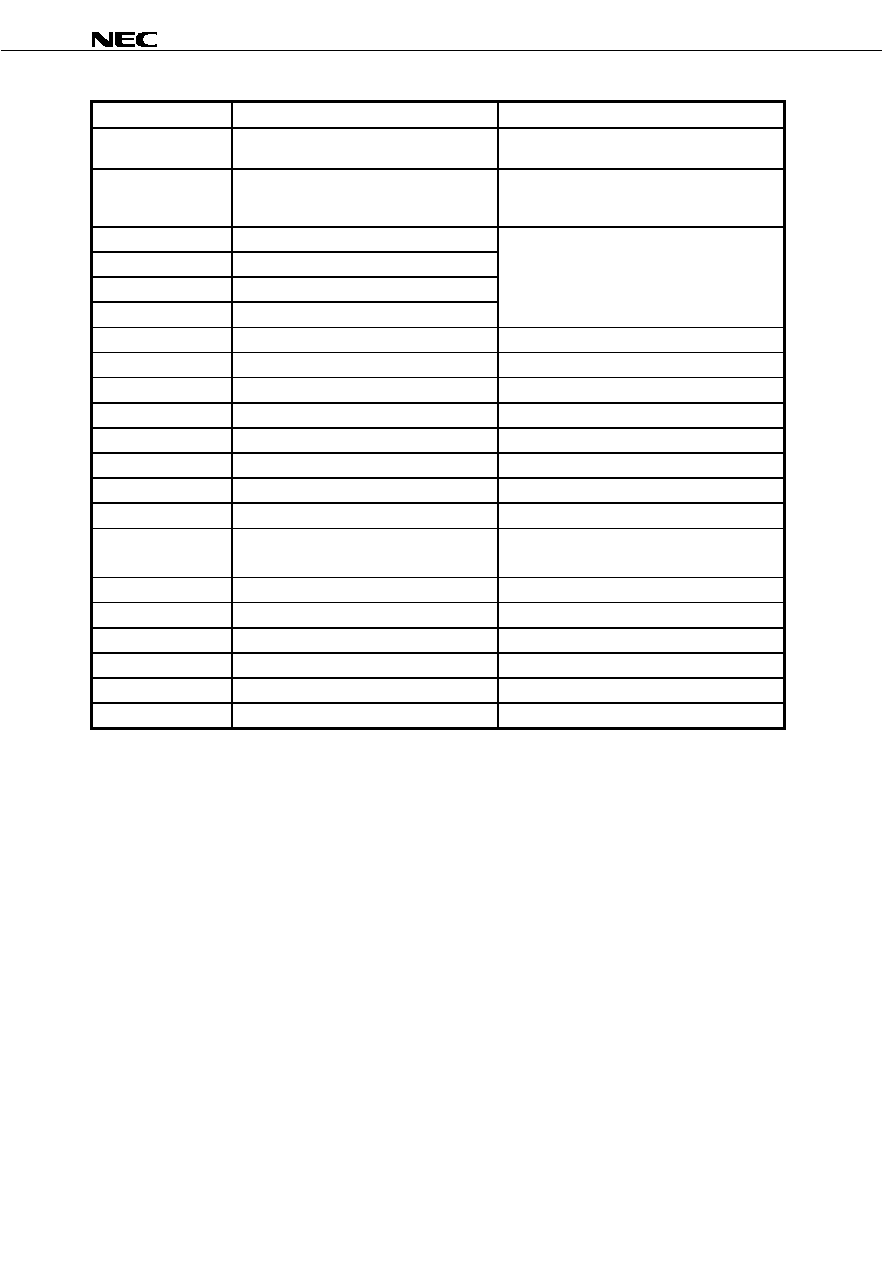
Pin Identification
Symbol
Pin No.
Description
A0 - A17
37, 36, 35, 34, 33, 32, 100, 99, 82, 81, 44, 45,
46, 47, 48, 49, 50, 43
Synchronous Address Input
I/O1 - I/O32
52, 53, 56, 57, 58, 59, 62, 63, 68, 69, 72, 73, 74,
75, 78, 79, 2, 3, 6, 7, 8, 9, 12, 13, 18, 19, 22, 23,
24, 25, 28, 29
Synchronous Data In,
Synchronous / Asynchronous Data Out
I/OP1, NC
Note
51
Synchronous Data In (Parity),
I/OP2, NC
Note
80
Synchronous / Asynchronous Data Out (Parity)
I/OP3, NC
Note
1
I/OP4, NC
Note
30
/ADV
83
Synchronous Burst Address Advance Input
/AP
84
Synchronous Address Status Processor Input
/AC
85
Synchronous Address Status Controller Input
/CE, CE2, /CE2
98, 97, 92
Synchronous Chip Enable Input
/BWE1 - /BWE4, /BWE
93, 94, 95, 96, 87
Synchronous Byte Write Enable Input
/GW
88
Synchronous Global Write Input
/G
86
Asynchronous Output Enable Input
CLK
89
Clock Input
MODE
31
Asynchronous Burst Sequence Select Input
Do not change state during normal operation
ZZ
64
Asynchronous Power Down State Input
V
DD
15, 41, 65, 91
Power Supply
V
SS
17, 40, 67, 90
Ground
V
DD
Q
4, 11, 20, 27, 54, 61, 70, 77
Output Buffer Power Supply
V
SS
Q
5, 10, 21, 26, 55, 60, 71, 76
Output Buffer Ground
NC
14, 16, 38, 39, 42, 66
No Connection
Note NC (No Connection) is used in the
Á
PD4382323GF. I/OP1 - I/OP4 is used in the
Á
PD4382363GF.


