The information in this document is subject to change without notice. Before using this document, please
confirm that this is the latest version.
Not all devices/types available in every country. Please check with local NEC representative for
availability and additional information.
©
2000
MOS INTEGRATED CIRCUIT
µ
PD23C128040AL
128M-BIT MASK-PROGRAMMABLE ROM
16M-WORD BY 8-BIT (BYTE MODE) / 8M-WORD BY 16-BIT (WORD MODE)
PAGE ACCESS MODE
DATA SHEET
Document No. M14824EJ2V0DS00 (2nd edition)
Date Published July 2001 NS CP (K)
Printed in Japan
The mark
5
5
5
5
shows major revised points.
Description
The
µ
PD23C128040AL is a 134,217,728 bits mask-programmable ROM. The word organization is selectable (BYTE
mode : 16,777,216 words by 8 bits, WORD mode : 8,388,608 words by 16 bits).
The active levels of OE (Output Enable Input) can be selected with mask-option.
The
µ
PD23C128040AL is packed in 48-pin PLASTIC TSOP(I).
Features
·
Word organization
16,777,216 words by 8 bits (BYTE mode)
8,388,608 words by 16 bits (WORD mode)
·
Page access mode
BYTE mode
: 8 byte random page access
WORD mode : 4 word random page access
·
Operating supply voltage : V
CC
=
2.7 to 3.6 V
Operating supply voltage Access time / Page access time Power supply current (Active mode) Standby current (CMOS level input)
V
CC
ns (MAX.)
mA (MAX.)
µ
A (MAX.)
3.3 V
±
0.3 V
100 / 25
70
30
3.0 V
±
0.3 V
120 / 25
65
Ordering Information
Part Number
Package
µ
PD23C128040ALGY-xxx-MJH
48-pin PLASTIC TSOP(I) (12x18) (Normal bent)
µ
PD23C128040ALGY-xxx-MKH
48-pin PLASTIC TSOP(I) (12x18) (Reverse bent)
(xxx : ROM code suffix No.)
Data Sheet M14824EJ2V0DS
2
µ
PD23C128040AL
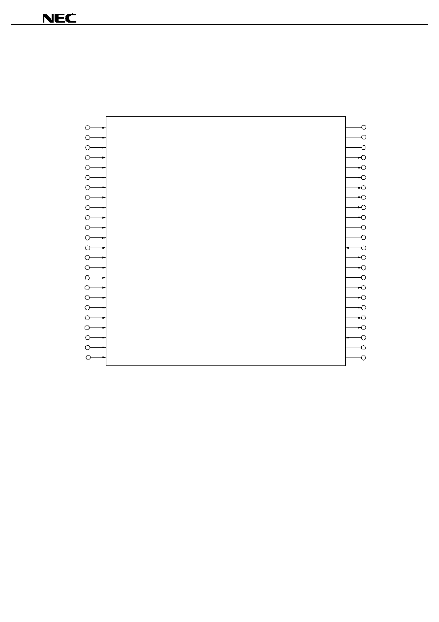
Pin Configurations (Marking Side)
/xxx indicates active low signal.
48-pin PLASTIC TSOP(I) (12 x 18) (Normal bent)
[
µ
µ
µ
µ
PD23C128040ALGY-xxx-MJH ]
WORD, /BYTE
A16
A15
A14
A13
A12
A11
A10
A9
A8
A19
A21
A20
A18
A17
A7
A6
A5
A4
A3
A2
A1
A0
/CE
GND
GND
O15, A1
O7
O14
O6
O13
O5
O12
O4
V
CC
V
CC
A22
O11
O3
O10
O2
O9
O1
O8
O0
/OE, OE, DC
GND
GND
1
2
3
4
5
6
7
8
9
10
11
12
13
14
15
16
17
18
19
20
21
22
23
24
48
47
46
45
44
43
42
41
40
39
38
37
36
35
34
33
32
31
30
29
28
27
26
25
A0 - A22
: Address inputs
O0 - O7, O8 - O14
: Data outputs
O15, A1
: Data output 15 (WORD mode),
LSB Address input (BYTE mode)
WORD, /BYTE
: Mode select
/CE
: Chip Enable
/OE, OE
: Output Enable
V
CC
: Supply voltage
GND
: Ground
DC
: Don't Care
Remark Refer to Package Drawings for the 1-pin index mark.

Data Sheet M14824EJ2V0DS
3
µ
PD23C128040AL
48-pin PLASTIC TSOP(I) (12 x 18) (Reverse bent)
[
µ
µ
µ
µ
PD23C128040ALGY-xxx-MKH ]
WORD, /BYTE
A16
A15
A14
A13
A12
A11
A10
A9
A8
A19
A21
A20
A18
A17
A7
A6
A5
A4
A3
A2
A1
A0
/CE
GND
GND
O15, A1
O7
O14
O6
O13
O5
O12
O4
V
CC
V
CC
A22
O11
O3
O10
O2
O9
O1
O8
O0
/OE, OE, DC
GND
GND
1
2
3
4
5
6
7
8
9
10
11
12
13
14
15
16
17
18
19
20
21
22
23
24
48
47
46
45
44
43
42
41
40
39
38
37
36
35
34
33
32
31
30
29
28
27
26
25
A0 - A22
: Address inputs
O0 - O7, O8 - O14
: Data outputs
O15, A1
: Data output 15 (WORD mode),
LSB Address input (BYTE mode)
WORD, /BYTE
: Mode select
/CE
: Chip Enable
/OE, OE
: Output Enable
V
CC
: Supply voltage
GND
: Ground
DC
: Don't Care
Remark Refer to Package Drawings for the 1-pin index mark.
Data Sheet M14824EJ2V0DS
4
µ
PD23C128040AL
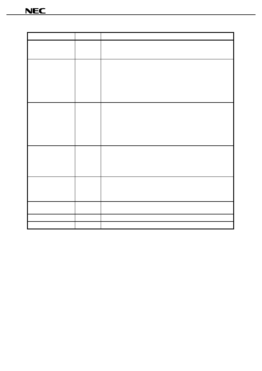
Input / Output Pin Functions
Pin name
Input / Output
Function
WORD, /BYTE
Input
The pin for switching WORD mode and BYTE mode.
High level : WORD mode (8M-word by 16-bit)
Low level : BYTE mode (16M-word by 8-bit)
A0 to A22
(Address inputs)
Input
Address input pins.
A0 to A22 are used differently in the WORD mode and the BYTE mode.
WORD mode (8M-word by 16-bit)
A0 to A22 are used as 23 bits address signals.
BYTE mode (16M-word by 8-bit)
A0 to A22 are used as the upper 23 bits of total 24 bits of address signal.
(The least significant bit (A
-
1) is combined to O15.)
O0 to O7, O8 to O14
(Data outputs)
Output
Data output pins.
O0 to O7, O8 to O14 are used differently in the WORD mode and the BYTE mode.
WORD mode (8M-word by 16-bit)
The lower 15 bits of 16 bits data outputs to O0 to O14.
(The most significant bit (O15) combined to A
-
1.)
BYTE mode (16M-word by 8-bit)
8 bits data outputs to O0 to O7 and also O8 to O14 are high impedance.
O15, A
-
1
(Data output 15,
LSB Address input)
Output, Input
O15, A
-
1 are used differently in the WORD mode and the BYTE mode.
WORD mode (8M-word by 16-bit)
The most significant output data bus (O15).
BYTE mode (16M-word by 8-bit)
The least significant address bus (A
-
1).
/CE
(Chip Enable)
Input
Chip activating signal.
When the OE is active, output states are following.
High level : High impedance
Low level : Data out
/OE, OE, DC
(Output Enable, Don't Care)
Input
Output enable signal. The active level of OE is mask option. The active level of OE
can be selected from high active, low active and Don't care at order.
V
CC
-
Supply voltage
GND
-
Ground

Data Sheet M14824EJ2V0DS
5
µ
PD23C128040AL
Block Diagram
O15, A1
WORD, /BYTE
/OE, OE, DC
/CE
Output Buffer
Y-Selector
Memory Cell Matrix
8,388,608 words by 16 bits /
16,777,216 words by 8 bits
Address Input Buffer
X-Decoder
Logic/Input
Input Buffer
Y-Decoder
A19
A18
A17
A16
A15
A14
A13
A12
A11
A10
A9
A8
A7
A6
A5
A4
A3
A2
A1
A0
O14
O13
O12
O11
O10
O9
O8
O0
O1
O2
O3
O4
O5
O6
O7
A20
A21
A22