
DATA SHEET
The information in this document is subject to change without notice. Before using this document, please
confirm that this is the latest version.
Not all devices/types available in every country. Please check with local NEC representative for
availability and additional information.
®
1997, 2000
Document No. P13103EJ3V0DS00 (3rd edition)
Date Published February 2000 NS CP(K)
Printed in Japan
PHOTOCOUPLER
PS9711
HIGH NOISE REDUCTION/HIGH-SPEED 10 Mbps, TOTEM-POLE OUTPUT TYPE
5-PIN SOP TOM PHOTOCOUPLER
-
NEPOC
TM
Series
-
The mark
À
À
À
À
shows major revised points.
DESCRIPTION
The PS9711 is an optically coupled high-speed, totem-pole output isolator containing a GaAlAs LED on light
emitting diode (input) and a photodiode and a signal processing circuit on light receiving side (output side) on one
chip.
FEATURES
À High common mode transient immunity (CM
H
, CM
L
=
▒
10 kV/
Á
s TYP.)
À Small package (5-pin SOP)
À High-speed response (t
PHL
= 30 ns, t
PLH
= 35 ns TYP.)
À Pulse width distortion (
t
PHL
¡ t
PLH
= 7 ns TYP.)
À Totem-pole output (No pull-up resistor required)
À Ordering number of taping product: PS9711-E3, E4: 900 pcs/reel,
PS9711-F3, F4 (Recommended): 3 500 pcs/reel
APPLICATIONS
À Computer and peripheral manufactures
À Measurement equipment
À PDP

Data Sheet P13103EJ3V0DS00
2
PS9711
PACKAGE DIMENSIONS (in millimeters)
1.27
0.4
+0.10
¡0.05
0.25 M
0.1▒0.1
2.1▒0.2
4.4
7.0▒0.3
0.5▒0.3
0.15
+0.10 ¡0.05
4.0▒0.5
1. Anode
2. Cathode
3. GND
4. V
O
5. V
CC
TOP VIEW
5
3
1
2
4
INTERNAL OUT PUT CIRCUIT
V
CC
(5)
Vo (4)
GND (3)
LED
Output
ON
L
OFF
H

Data Sheet P13103EJ3V0DS00
3
PS9711
ORDERING INFORMATION
Part Number
Package
Packing Style
Application Part Number
*1
PS9711
5-pin SOP
Magazine case 100 pcs
PS9711
PS9711-E3
Embossed Tape 900 pcs/reel
PS9711-E4
PS9711-F3
Embossed Tape 3 500 pcs/reel
PS9711-F4
*1 For the application of the Safety Standard, following part number should be used.
ABSOLUTE MAXIMUM RATINGS (T
A
= 25
░
░
░
░
C, unless otherwise specified)
Parameter
Symbol
Ratings
Unit
Diode
Forward Current
I
F
30
mA
Reverse Voltage
V
R
3.0
V
Detector
Supply Voltage
V
CC
7
V
Output Voltage
V
O
7
V
High Level Output Current
*1
I
OH
-
5
mA
Low Level Output Current
*1
I
OL
13
mA
Power Dissipation
*1
P
C
130
mW
Isolation Voltage
*2
BV
2 500
Vr.m.s.
Operating Ambient Temperature
T
A
-
40 to +85
░
C
Storage Temperature
T
stg
-
55 to +125
░
C
*1 T
A
=
-
40 to +85
░
C
*2 AC voltage for 1 minute at T
A
= 25
░
C, RH = 60 % between input and output.
RECOMMENDED OPERATING CONDITIONS
Parameter
Symbol
MIN.
TYP.
MAX.
Unit
High Level Input Current
I
FH
7.5
12.5
mA
Low Level Input Current
I
FL
0
250
Á
A
Supply Voltage
V
CC
4.5
5.0
5.5
V
TTL (loads)
N
3

Data Sheet P13103EJ3V0DS00
4
PS9711
ELECTRICAL CHARACTERISTICS (T
A
=
-
-
-
-
40 to +85 ░C, unless otherwise specified)
Parameter
Symbol
Conditions
MIN.
TYP.
*1
MAX.
Unit
Diode
Forward Voltage
V
F
I
F
= 10 mA, T
A
= 25
░
C
1.4
1.65
1.9
V
Reverse Current
I
R
V
R
= 3 V, T
A
= 25
░
C
10
Á
A
Terminal Capacitance
C
t
V = 0 V, f = 1 MHz, T
A
= 25
░
C
30
pF
Detector
High Level Output Current
I
OH
V
CC
= V
O
= 5.5 V, I
F
= 250
Á
A
1
200
Á
A
High Level Output Voltage
V
OH
V
CC
= 4.5 V, I
F
= 250
Á
A, I
OH
=
-
2 mA
2.4
3.0
V
Low Level Output Voltage
V
OL
V
CC
= 4.5 V, I
F
= 7 mA, I
O
= 8 mA
0.38
0.6
V
High Level Supply Current
I
CCH
V
CC
= 5.5 V, I
F
= 0 mA
11
17
mA
Low Level Supply Current
I
CCL
V
CC
= 5.5 V, I
F
= 10 mA
12
18
mA
High Level Output Short
Circuit Current
I
OSH
V
CC
= 5.5 V, V
O
= GND, I
F
= 0 mA,
10 ms or less
¡26
mA
Low Level Output Short
Circuit Current
I
OSL
V
CC
= V
O
= 5.5 V, I
F
= 8 mA,
10 ms or less
34
mA
Coupled
Threshold Input Current
I
FHL
V
CC
= 5 V
T
A
= 25
░
C
2.0
5
mA
(H
L)
6
Threshold Input Current
I
FLH
V
CC
= 5 V
T
A
= 25
░
C
0.5
mA
(L
H)
0.35
Isolation Resistance
R
I-O
V
I-O
= 1 kV
DC
, RH = 40 to 60 %,
T
A
= 25
░
C
10
11
Isolation Capacitance
C
I-O
V = 0 V, f = 1 MHz, T
A
= 25
░
C
0.4
pF
Propagation Delay Time
t
PHL
T
A
= 25
░
C
15
30
65
ns
(H
L)
*2
V
CC
= 5 V, I
F
= 7.5 mA
10
85
Propagation Delay Time
t
PLH
T
A
= 25
░
C
15
35
65
ns
(L
H)
*2
V
CC
= 5 V, I
F
= 7.5 mA
10
85
Pulse Width Distortion
(PWD)
*2
t
PHL-
t
PLH
V
CC
= 5 V, I
F
= 7.5 mA
7
35
ns
Common Mode
Transient Immunity at High
Level Output
*3
CM
H
V
CC
= 5 V, T
A
= 25
░
C, I
F
= 0 mA,
V
O (MIN.)
= 2 V, V
CM
= 100 V
1
10
kV/
Á
s
Common Mode
Transient Immunity at Low
Level Output
*3
CM
L
V
CC
= 5 V, T
A
= 25
░
C, I
F
= 7.5 mA,
V
O (MAX.)
= 0.8 V, V
CM
= 100 V
1
10
kV/
Á
s
Data Sheet P13103EJ3V0DS00
5
PS9711
*1 Typical values at T
A
= 25
░
C
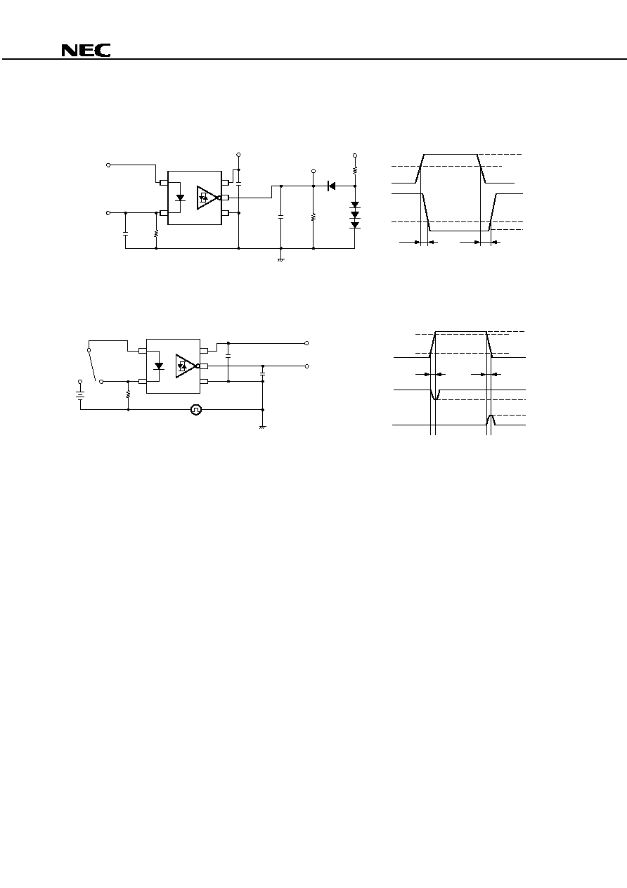
*2 Test circuit for propagation delay time
Input
Output
1.5 V
V
OH
V
OL
t
PHL
t
PLH
I
F
(ON)
50 % I
F
(ON)
C
L
is approximately which includes probe and stray wiring capacitance.
47
Pulse input (I
F
)
V
O
(monitor)
V
CC
= 5 V
Input
(monitor)
0.1 F
Á
C
L
=
30 pF
C
L
= 15 pF
GND
V
CC
2.5 k
1.3 k
(PW = 500 ns,
Duty cycle = 1/2)
V
CC
= 5 V
*3 Test circuit for common mode transient immunity
90 %
10 %
100 V
0 V
V
OH
2 V
0.8 V
V
OL
V
CM
V
O
(I
F
= 0 mA)
V
O
(I
F
= 7.5 mA)
t
r
t
f
C
L
is approximately which includes probe and stray wiring capacitance.
V
O
(Monitor)
V
CC
= 5 V
0.1 F
Á
C
L
= 15 pF
GL SW I
F
GND
V
CC
USAGE CAUTIONS
1. This product is weak for static electricity by designed with high-speed integrated circuit so protect against static
electricity when handling.
2. By-pass capacitor of more than 0.1
Á
F is used between V
CC
and GND near device.