DATA SHEET
The information in this document is subject to change without notice. Before using this document, please confirm that
this is the latest version.
Not all devices/types available in every country. Please check with local NEC Compound Semiconductor Devices
representative for availability and additional information.
PHOTOCOUPLER
PS9113
1 Mbps, OPEN COLLECTOR OUTPUT
HIGH CMR, INTELLIGENT POWER MODULE
5-PIN SOP PHOTOCOUPLER
-
NEPOC Series
-
DESCRIPTION
The PS9113 is an optically coupled isolator containing a GaAlAs LED on the input side and a photo diode and a
signal processing circuit on the output side on one chip.
The PS9113 is specified high CMR, high CTR and pulse width distortion with operating temperature. It is suitable
for IPM drive.
FEATURES
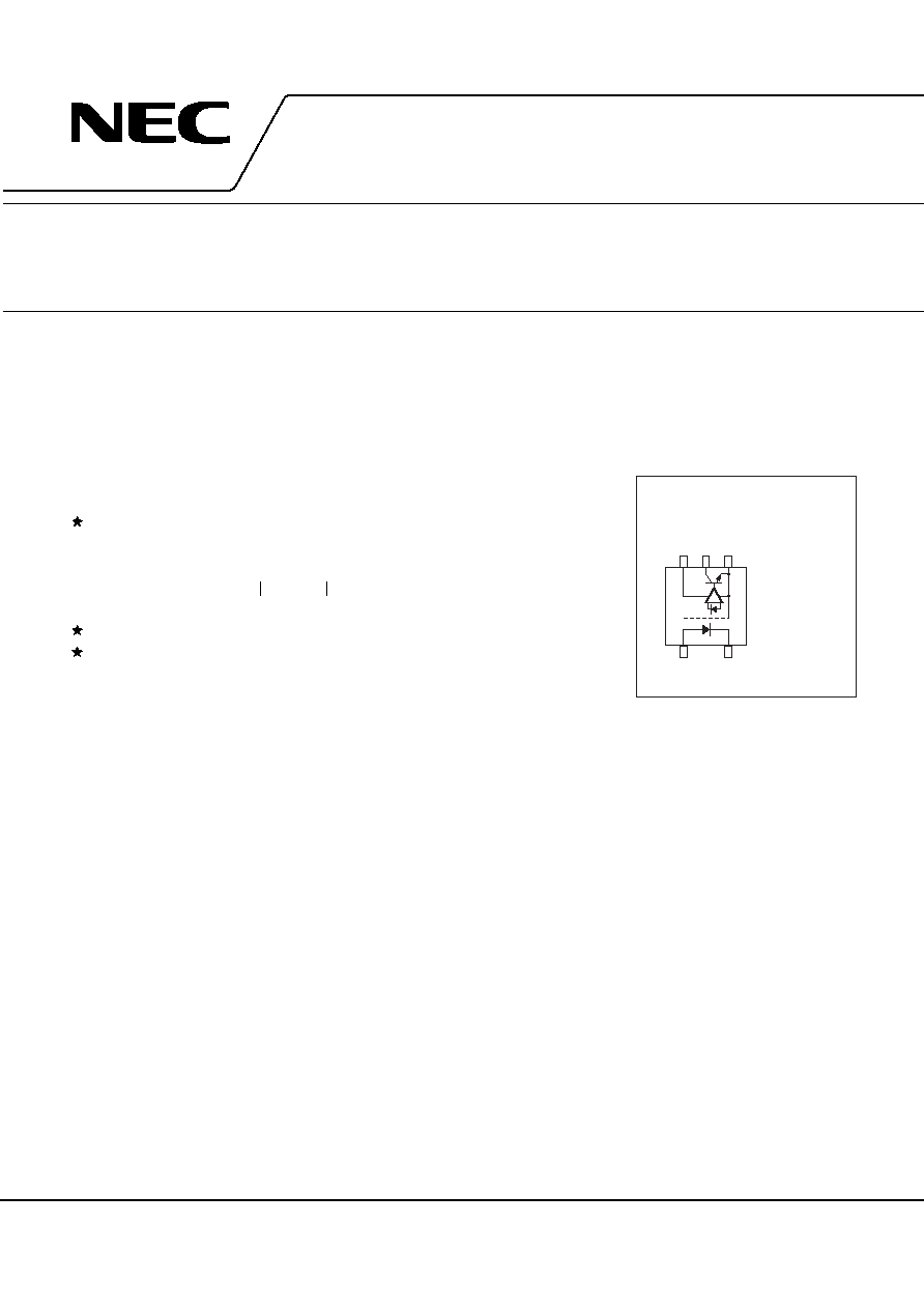
PIN CONNECTION
1. Anode
2. Cathode
3. GND
4. V
O
5. V
CC
(Top View)
5
3
1
2
4
· High instantaneous common mode rejection voltage (CM
H
, CM
L
=
±
15 kV/
µ
s MIN.)
· Small package (5-pin SOP)
· High-speed response (t
PHL
= 500 ns MAX., t
PLH
= 750 ns MAX.)
· Maximum propagation delays (t
PLH
-
t
PHL
= 270 ns TYP.)
· Pulse width distortion ( t
PHL
-
t
PLH
= 270 ns TYP.)
· Ordering number of taping product: PS9113-F3, F4: 2 500 pcs/reel
· Pb-Free
product
· Safety
standards
· UL approved: File No. E72422
· DIN EN60747-5-2 (VDE0884 Part2) approved: No. 40008902 (Option)
APPLICATIONS
· IPM
Driver
· General purpose inverter
Document No. PN10265EJ02V0DS (2nd edition)
Date Published February 2005 CP(K)
Printed in Japan
©
NEC Compound Semiconductor Devices, Ltd. 2003, 2005
The mark shows major revised points.
PS9113
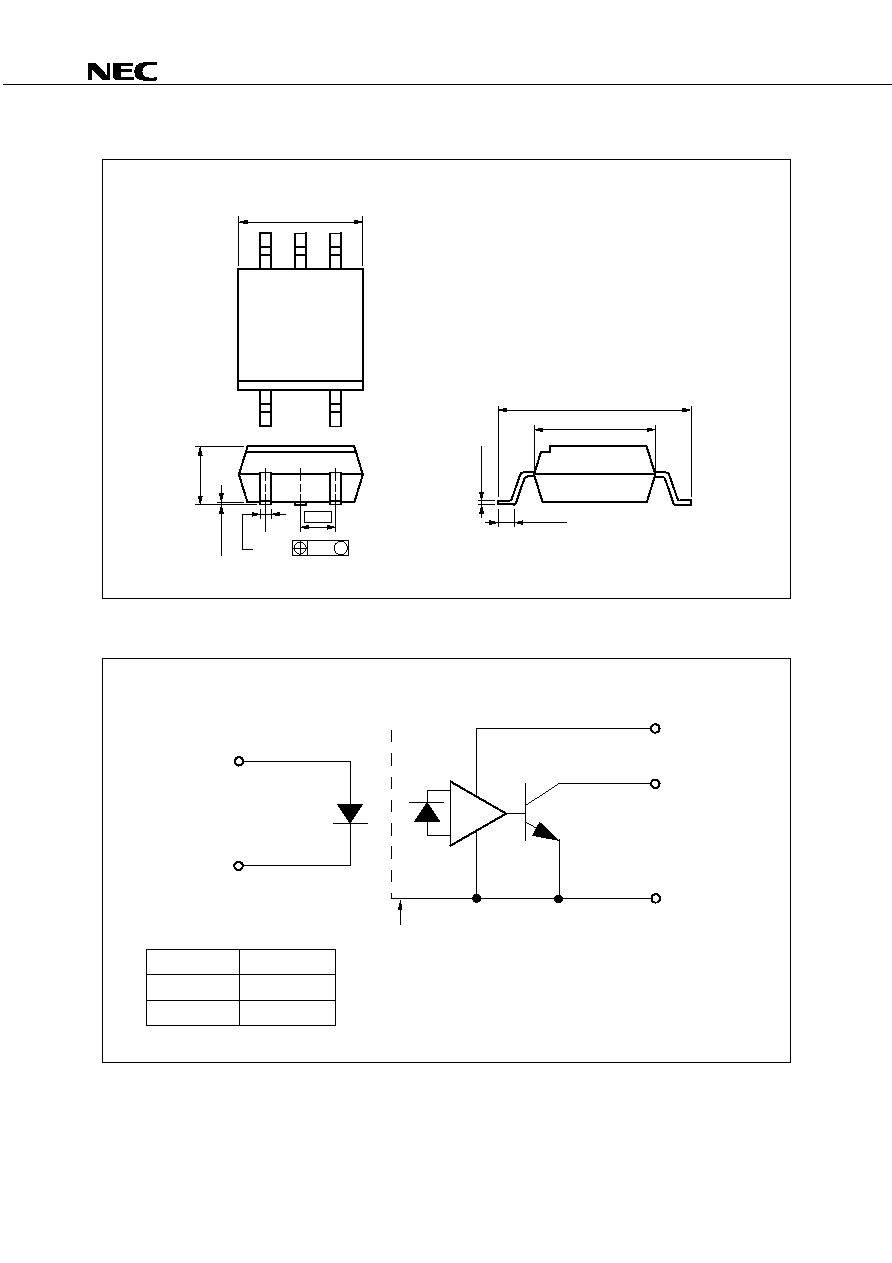
PACKAGE DIMENSIONS (UNIT: mm)
1.27
0.4
+0.10
0.05
0.25 M
0.1±0.1
2.6±0.2
4.4
7.0±0.3
0.5±0.3
0.15
+0.10 0.05
3.4
+0.3
0.1
FUNCTIONAL DIAGRAM
5
4
3
1
2
LED
Output
ON
L
OFF
H
Shield
Data Sheet PN10265EJ02V0DS
2

PS9113
MARKING EXAMPLE
No. 1 pin Mark
Initial of NEC
(Engraved mark)
Rank Code
Year Assembled
(Last 1 Digit)
Week Assembled
N
2
34
Assembly Lot
9113
N234
N
*1
*1 Bar : Pb-Free
Data Sheet PN10265EJ02V0DS
3
PS9113
ORDERING INFORMATION
Part Number
Order Number
Solder Plating
Specification
Packing Style
Safety Standard
Approval
Application
Part
Number
*1
PS9113 PS9113-A Pb-Free
*2
Magazine case 100 pcs
Standard products
PS9113
PS9113-F3
PS9113-F3-A
Embossed Tape 2500 pcs/reel
(UL approved)
PS9113-F4 PS9113-F4-A
PS9113-V
PS9113-V-A
Magazine case 100 pcs
DIN EN60747-5-2
PS9113-V-F3
PS9113-V-F3-A
Embossed Tape 2 500 pcs/reel (VDE0884 Part2)
PS9113-V-F4 PS9113-V-F4-A
Approved
(Option)
*1 For the application of the Safety Standard, following part number should be used.
*2 With regards to terminal solder (the solder contains lead) plated products (conventionally plated), contact your
nearby sales office.
ABSOLUTE MAXIMUM RATINGS (T
A
= 25
°
C, unless otherwise specified)
Parameter Symbol
Ratings
Unit
Diode Forward
Current
*1
I
F
25 mA
Reverse
Voltage
V
R
5 V
Detector Supply Voltage
V
CC
-
0.5 to +35
V
Output
Voltage
V
O
-
0.5 to +35
V
Output
Current
I
O
15 mA
Power
Dissipation
*2
P
C
100 mW
Isolation Voltage
*3
BV 2
500
Vr.m.s.
Operating Ambient Temperature
T
A
-
40 to +100
°
C
Storage Temperature
T
stg
-
55 to +125
°
C
*1 Reduced to 0.33 mA/
°
C at T
A
= 70
°
C or more.
*2 Reduced to 1.9 mW/
°
C at T
A
= 70
°
C or more.
*3 AC voltage for 1 minute at T
A
= 25
°
C, RH = 60% between input and output.
Pins 1-2 shorted together, 3-4 shorted together.
RECOMMENDED OPERATING CONDITIONS
Parameter Symbol
MIN.
TYP.
MAX.
Unit
High Level Input Current
I
FH
10 20 mA
Output Voltage
V
O
0 30 V
Supply Voltage
V
CC
4.5 30 V
LED Off Voltage
V
F
0 0.8 V
Data Sheet PN10265EJ02V0DS
4
PS9113
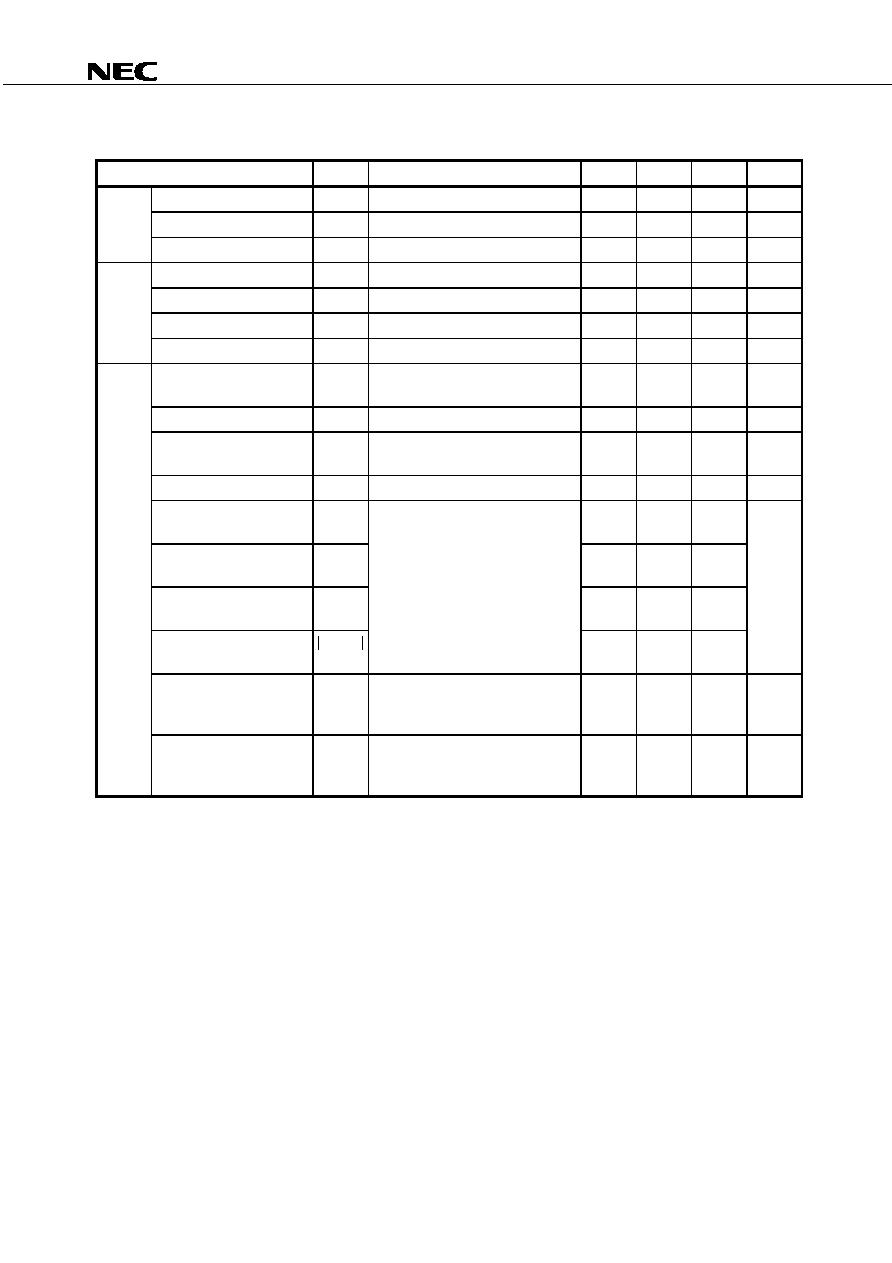
ELECTRICAL CHARACTERISTICS (T
A
=
-
40 to +100
°
C, V
CC
= 15 V, unless otherwise specified)
Parameter Symbol Conditions MIN.
TYP.
*1
MAX. Unit
Diode Forward
Voltage
V
F
I
F
= 10 mA
1.3
1.65
2.1
V
Reverse
Current
I
R
V
R
= 3 V
200
µ
A
Terminal
Capacitance C
t
V = 0 V, f = 1 MHz, T
A
= 25
°
C
30
pF
Detector Low Level Output Voltage
V
OL
I
F
= 10 mA, I
OL
= 2.4 mA
0.13
0.6
V
High Level Output Current
I
OH
V
CC
= V
O
= 30 V, V
F
= 0.8 V
0.01
50
µ
A
High Level Supply Current
I
CCH
V
CC
= 30 V, V
F
= 0.8 V, V
O
= open
0.6
1.3
mA
Low Level Supply Current
I
CCL
V
CC
= 30 V, I
F
= 10 mA, V
O
= open
0.6
1.3
mA
Coupled Threshold Input Current
(H
L)
I
FHL
V
O
= 0.8 V, I
O
= 0.75 mA
1.5
5.0
mA
Current Transfer Ratio (I
C
/I
F
) CTR I
F
= 10 mA, V
O
= 0.6 V
44
110
%
Isolation
Resistance R
I-O
V
I-O
= 1 kV
DC
, RH = 40 to 60%,
T
A
= 25
°
C
10
11
Isolation
Capacitance C
I-O
V = 0 V, f = 1 MHz, T
A
= 25
°
C
0.6 pF
Propagation Delay Time
(H
L)
*2
t
PHL
I
F
= 10 mA, R
L
= 20 k
, C
L
= 100 pF,
V
THHL
= 1.5 V, V
THLH
= 2.0 V
250
500 ns
Propagation Delay Time
(L
H)
*2
t
PLH
520
750
Maximum
Propagation
Delays
t
PLH
-
t
PHL
-
200 270 650
Pulse Width Distortion
(PWD)
*2
t
PHL-
t
PLH
270
650
Common Mode
Transient Immunity at High
Level Output
*3
CM
H
T
A
= 25
°
C, I
F
= 0 mA, V
O
> 3.0 V,
V
CM
= 1.5 kV, R
L
= 20 k
,
C
L
= 100 pF
15
kV/
µ
s
Common Mode
Transient Immunity at Low
Level Output
*3
CM
L
T
A
= 25
°
C, I
F
= 10 mA, V
O
< 1.0 V,
V
CM
= 1.5 kV, R
L
= 20 k
,
C
L
= 100 pF
15
kV/
µ
s
Data Sheet PN10265EJ02V0DS
5