DATA SHEET
The information in this document is subject to change without notice. Before using this document, please
confirm that this is the latest version.
Not all devices/types available in every country. Please check with local NEC representative for
availability and additional information.
®
1988, 1999
Document No. P11311EJ5V0DS00 (5th edition)
Date Published February 1999 NS CP(K)
Printed in Japan
PHOTOCOUPLER
PS2707-1,PS2707-2,PS2707-4
AC INPUT RESPONSE
HIGH COLLECTOR TO EMITTER VOLTAGE TYPE
SOP MULTI PHOTOCOUPLER SERIES
The mark
À
À
À
À
shows major revised points.
-
NEPOC
TM
Series
-
DESCRIPTION
The PS2707-1, PS2707-2, PS2707-4 are optically coupled isolators containing GaAs light emitting diodes and an
NPN silicon phototransistor.
Each is mounted in a plastic SOP (Small Outline Package) for high density applications.
This package has shield effect to cut off ambient light.
FEATURES
À AC input response
À High collector to emitter voltage (V
CEO
= 120 V)
À High isolation voltage (BV = 3 750 Vr.m.s.)
À Small and thin (SOP) package
À High-speed switching (t
r
, t
f
= 10
Á
s TYP.)
À Ordering number of taping product (1-ch only): PS2707-1-E3, E4, F3, F4
À UL approved: File No. E72422 (S)
À VDE0884 approved (Option)
APPLICATIONS
À Hybrid IC
À Telephone/FAX
À FA/OA equipment
À Programmable logic controllers
ORDERING INFORMATION
Part Number
Package
Safety Standard Approval
PS2707-1
4-pin SOP
Standard specification products
PS2707-2
8-pin SOP
À UL approved
PS2707-4
16-pin SOP
PS2707-1-V
4-pin SOP
VDE0884 specification products (Option)
PS2707-2-V
8-pin SOP
PS2707-4-V
16-pin SOP
Data Sheet P11311EJ5V0DS00
2
PS2707-1,PS2707-2,PS2707-4
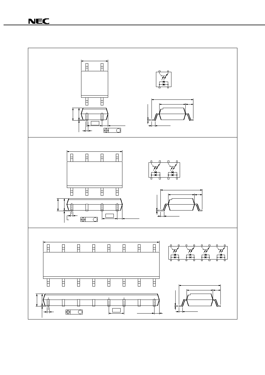
PACKAGE DIMENSIONS (in millimeters)
PS2707-1
4.5 MAX.
7.0▒0.3
4.4
1.3
0.5▒0.3
0.15
+0.10 ¡0.05
2.0
0.1▒0.1
2.3 MAX.
2.54
1.2 MAX.
0.4
+0.10
¡0.05
0.25 M
PS2707-2
9.3 MAX.
2.0
0.1▒0.1
2.3 MAX.
2.54
1.2 MAX.
0.4
+0.10
¡0.05
0.25 M
7.0▒0.3
4.4
1.3
0.5▒0.3
0.15
+0.10 ¡0.05
PS2707-4
19.46 MAX.
2.0
0.1▒0.1
2.3 MAX.
2.54
1.2 MAX.
0.4
+0.10
¡0.05
0.25 M
7.0▒0.3
4.4
1.3
0.5▒0.3
0.15
+0.10 ¡0.05
TOP VIEW
1. Anode, Cathode
2. Cathode, Anode
3. Emitter
4. Collector
4
3
1
2
TOP VIEW
1
2
3
4
8
7
6
5
1. 3. Anode, Cathode
2. 4. Cathode, Anode
5. 7. Emitter
6. 8. Collector
TOP VIEW
1. 3. 5. 7. Anode, Cathode
2. 4. 6. 8. Cathode, Anode
9. 11. 13. 15. Emitter
10. 12. 14. 16. Collector
16
15
14
13
12
11
10
9
1
2
3
4
5
6
7
8
Data Sheet P11311EJ5V0DS00
3
PS2707-1,PS2707-2,PS2707-4
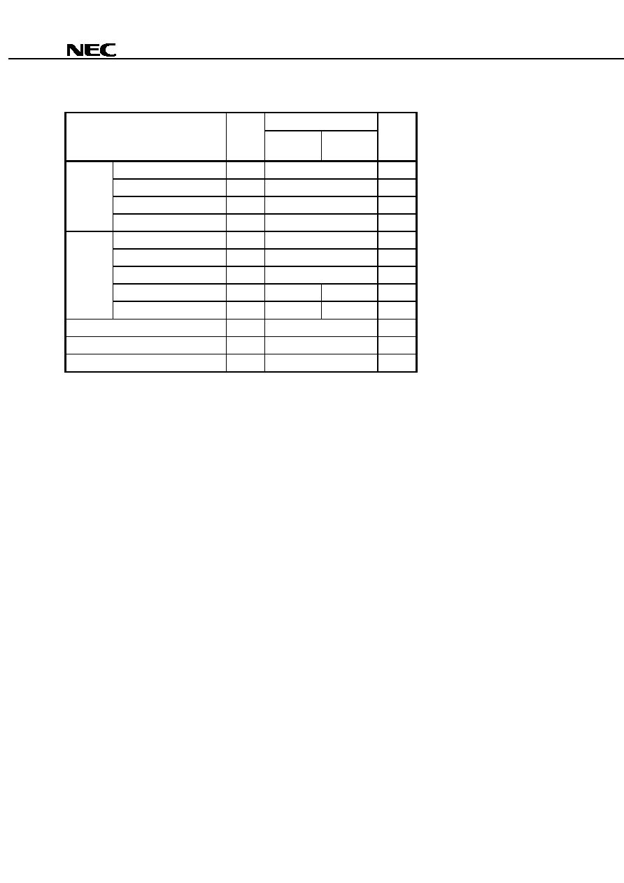
ABSOLUTE MAXIMUM RATINGS (T
A
= 25
░
░
░
░
C, unless otherwise specified)
Ratings
Parameter
Symbol
PS2707-1
PS2707-2,
PS2707-4
Unit
Diode
Forward Current (DC)
I
F
▒
50
mA
Power Dissipation Derating
P
D
/
░
C
0.8
mW/
░
C
Power Dissipation
P
D
80
mW/ch
Peak Forward Current
*1
I
FP
▒
1
A
Transistor
Collector to Emitter Voltage
V
CEO
120
V
Emitter to Collector Voltage
V
ECO
6
V
Collector Current
I
C
30
mA/ch
Power Dissipation Derating
P
C
/
░
C
1.5
1.2
mW/
░
C
Power Dissipation
P
C
150
120
mW/ch
Isolation Voltage
*2
BV
3 750
Vr.m.s.
Operating Ambient Temperature
T
A
¡55 to +100
░
C
Storage Temperature
T
stg
¡55 to +150
░
C
*1 PW = 100
Á
s, Duty Cycle = 1 %
*2 AC voltage for 1 minute at T
A
= 25 ░C, RH = 60 % between input and output
Data Sheet P11311EJ5V0DS00
4
PS2707-1,PS2707-2,PS2707-4
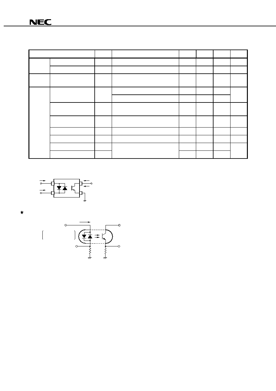
ELECTRICAL CHARACTERISTICS (T
A
= 25
░
░
░
░
C)
Parameter
Symbol
Conditions
MIN.
TYP.
MAX.
Unit
Diode
Forward Voltage
V
F
I
F
=
▒
5 mA
1.1
1.4
V
Terminal Capacitance
C
t
V = 0 V, f = 1 MHz
60
pF
Transistor
Collector to Emitter
Current
I
CEO
I
F
= 0 mA, V
CE
= 120 V
100
nA
Coupled
CTR
I
F
=
▒
5 mA, V
CE
= 5 V
50
150
400
%
Current Transfer Ratio
(I
C
/I
F
)
I
F
=
▒
1 mA, V
CE
= 5 V
10
80
CTR Ratio
*1
CTR1/
CTR2
I
F
=
▒
5 mA, V
CE
= 5 V
0.3
1.0
3.0
Collector Saturation
Voltage
V
CE (sat)
I
F
=
▒
10 mA, I
C
= 2 mA
0.3
V
Isolation Resistance
R
I-O
V
I-O
= 1 kV
DC
10
11
Isolation Capacitance
C
I-O
V = 0 V, f = 1 MHz
0.4
pF
Rise Time
*2
t
r
V
CC
= 5 V, I
C
= 2 mA, R
L
= 1 k
10
Á
s
Fall Time
*2
t
f
10
*1 CTR1 = I
C1
/I
F1
, CTR2 = I
C2
/I
F2
I
F1
I
F2
I
C1
I
C2
V
CE
*2 Test circuit for switching time
V
CC
V
OUT
R
L
= 1 k
PW = 100 s
Duty Cycle = 1/10
Á
I
F
Pulse Input
50
Input monitor
Data Sheet P11311EJ5V0DS00
5
PS2707-1,PS2707-2,PS2707-4
TYPICAL CHARACTERISTICS (T
A
= 25 ░C, unless otherwise specified)
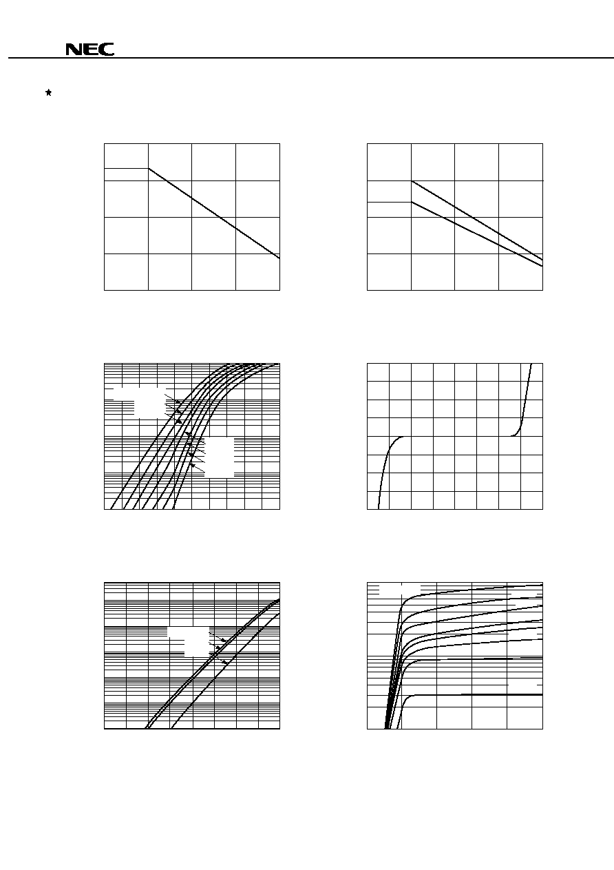
100
50
25
0
75
25
50
75
100
Ambient Temperature T
A
(░C)
Diode Power Dissipation P
D
(mW)
DIODE POWER DISSIPATION vs.
AMBIENT TEMPERATURE
200
150
100
50
0
25
50
75
100
Ambient Temperature T
A
(░C)
Transistor Power Dissipation P
C
(mW)
TRANSISTOR POWER DISSIPATION vs.
AMBIENT TEMPERATURE
PS2707-1
1.5 mW/░C
PS2707-2,
PS2707-4
1.2 mW/░C
100
0.1
1
0.01
10
0.6
1.0
1.4
1.6
0.8
1.2
Forward Voltage V
F
(V)
Forward Current I
F
(mA)
FORWARD CURRENT vs.
FORWARD VOLTAGE
+25 ░C
0 ░C
¡25 ░C
¡55 ░C
T
A
= +100 ░C
+75 ░C
+50 ░C
FORWARD CURRENT vs.
FORWARD VOLTAGE
Forward Voltage V
F
(V)
Forward Current I
F
(mA)
80
60
40
20
0
¡40
¡60
¡80
¡20
¡1.2
0
0.4
1.2
1.6
¡1.6
¡0.8 ¡0.4
0.8
50 000
0.1
500
5 000
10
10 000
1 000
100
50
5
1
0.5
¡60
0
40
80
¡40
¡20
20
60
100
Ambient Temperature T
A
(░C)
COLLECTOR TO EMITTER DARK
CURRENT vs. AMBIENT TEMPERATURE
Collector to Emitter Dark Current I
CEO
(nA)
V
CE
= 40 V
24 V
10 V
10
0.1
0.5
5
1
0.2
0.6
1.0
0.0
0.4
0.8
Collector Saturation Voltage V
CE (sat)
(V)
Collector Current I
C
(mA)
COLLECTOR CURRENT vs.
COLLECTOR SATURATION VOLTAGE
I
F
= 25 mA
1.5 mA
1 mA
0.5 mA
10 mA
5 mA
2.5 mA
2 mA