
ę
1996
DATA SHEET
SILICON TRANSISTOR
2SC4186
DESCRIPTION
The 2SC4186 is an NPN silicon epitaxial transistor intended for use
as a UHF oscillator and a mixer in a tuner of a TV receiver. The device
features stable oscillation and small frequency drift against any change
of the supply voltage and the ambient temperature.
It is designed for use in small type equipments especially recom-
mended for Hybrid Integrated Circuit and other applications.
FEATURES
Ě
High Gain Bandwidth Product
: f
T
= 4.0 GHz.
Ě
Low Collector to Base Time Constant : C
C
Ě
r
b'b
= 4.0 ps TYP.
Ě
Low Output Capacitance
: C
ob
= 1.5 pF MAX.
ABSOLUTE MAXIMUM RATINGS (T
A
= 25 ░C)
Collector to Base Voltage
V
CB0
25
V
Collector to Emitter Voltage
V
CE0
12
V
Emitter to Base Voltage
V
EB0
3.0
V
Collector Current
I
C
30
mA
Total Power Dissipation
P
T
160
mW
Junction Temperature
T
j
150
░C
Storage Temperature
T
stg
ş65 to +150
░C
ELECTRICAL CHARACTERISTICS (T
A
= 25 ░C)
Characteristics
Symbol
MIN.
TYP.
MAX.
Unit
Test Conditions
Collector Cutoff Current
I
CB0
0.1
Á
A
V
CB
= 15 V, I
E
= 0
DC Current Gain
h
FE
40
100
200
V
CE
= 10 V, I
C
= 5 mA
Collector Saturation Voltage
V
CE(sat)
0.09
0.5
V
I
C
= 10 mA, I
B
= 1.0 mA
Gain Bandwidth Product
f
T
2.5
4.0
GHz
V
CE
= 10 V, I
C
= 5 mA, f = 1 GHz
Output Capacitance
C
ob
1.0
1.8
pF
V
CB
= 10 V, I
E
= 0, f = 1 MHz
Collector to Base Time Constant
C
c
Ě r
b'b
5.0
ps
V
CE
= 10 V, I
E
= ş5 mA, f = 31.9 MHz
h
FE
Classifications
Rank
T62
T63
T64
Marking
T62
T63
T64
h
FE
40 to 80
60 to 120
100 to 200
Document No. P11191EJ2V0DS00 (2nd edition)
Date Published February 1996 P
Printed in Japan
UHF OSCILLATOR AND UHF MIXER
NPN SILICON EPITAXIAL TRANSISTOR
MINI MOLD
PACKAGE DIMENSIONS
in millimeters
2.1 ▒ 0.1
1.25 ▒ 0.1
2
1
3
2.0 ▒ 0.2
0.3
+0.1
ş0
0.65
0.65
0.3
+0.1
ş0
0.15
+0.1
ş0.05
0 to 0.1
0.3
0.9 ▒ 0.1
Marking
PIN CONNECTIONS
1. Emitter
2. Base
3. Collector
2SC4186
2
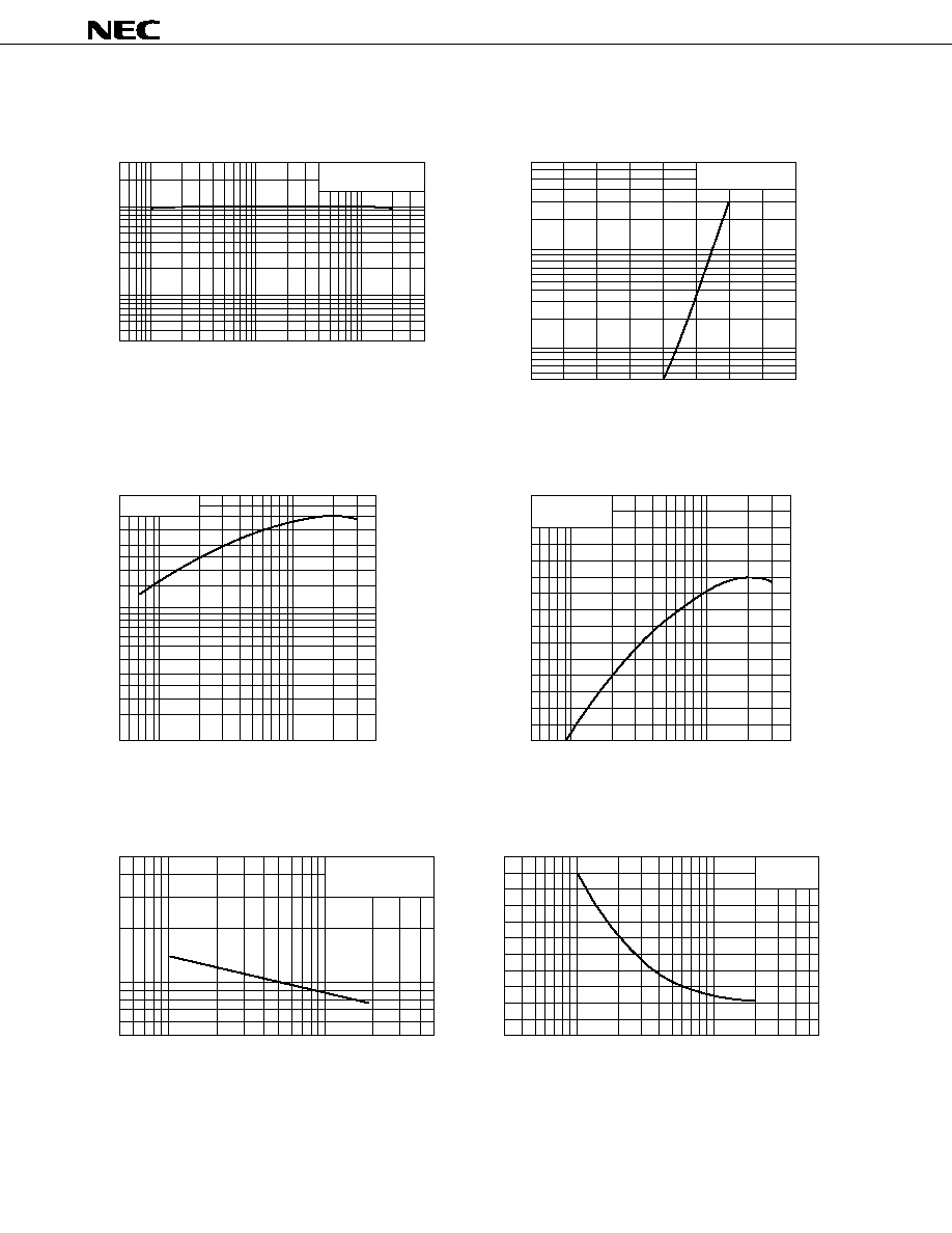
TYPICAL CHARACTERISTICS (T
A
= 25 ░C)
200
100
10
20
50
5
0.05
0.2
1
0.1
0.5
2
5
10
20
40
I
C
- Collector Current - mA
h
FE
- DC Current Gain
V
CE
= 10 V
70
50
20
10
2
5
1
0.5
0.6
0.7
0.8
0.9
V
CE
= 10 V
V
BE
- Base to Emitter Voltage - V
I
C
- Collector Current - mA
COLLECTOR CURRENT vs.
BASE TO EMITTER VOLTAGE
7
5
2
1
0.5
0.2
0.1
0.5
1
2
5
10
20
40
f
T
- Gain Bandwidth Product - GHz
V
CE
= 10 V
GAIN BANDWIDTH PRODUCT vs.
COLLECTOR CURRENT
I
C
- Collector Current - mA
15
10
5
0
0.5
1
2
5
10
20
40
S
21e
2
- Insertion Gain - dB
V
CE
= 10 V
f = 1.0 GHz
INSERTION GAIN vs.
COLLECTOR CURRENT
I
C
- Collector Current - mA
3
2
1
0.5
C
ob
- Output Capacitance - pF
1
2
5
10
20
V
CB
- Collector to Base Voltage - V
f = 1.0 MHz
OUTPUT CAPACITANCE vs.
COLLECTOR TO BASE VOLTAGE
10
8
6
4
2
0
C
C
Ě r
b'b
- Collector to Base Time Constant - ps
0.5
1
5
50
20
I
C
- Collector Current - mA
V
CE
= 10 V
I
E
= ş5.0 mA
f = 39.1 MHz
C
C
Ě r
b' b
vs.
COLLECTOR CURRENT
2
10
DC CURRENT GAIN vs.
COLLECTOR CURRENT

2SC4186
3
T
A
- Ambient Temperature - ░C
P
T
- Total Power Dissipation - mW
Free Air
200
150
100
50
0
50
100
150
TOTAL POWER DISSIPATION vs.
AMBIENT TEMPERATURE

